1814 데이터 시트보기 (PDF) - Linear Technology
부품명
상세내역
제조사
1814 Datasheet PDF : 16 Pages
| |||
FEATURES
■ 100MHz Gain Bandwidth Product
■ 750V/µs Slew Rate
■ 3.6mA Maximum Supply Current per Amplifier
■ Tiny 3mm x 3mm x 0.8mm DFN Package
■ 8nV/√Hz Input Noise Voltage
■ Unity-Gain Stable
■ 1.5mV Maximum Input Offset Voltage
■ 4µA Maximum Input Bias Current
■ 400nA Maximum Input Offset Current
■ 40mA Minimum Output Current, VOUT = ±3V
■ ±3.5V Minimum Input CMR, VS = ±5V
■ 30ns Settling Time to 0.1%, 5V Step
■ Specified at ±5V, Single 5V Supplies
■ Operating TempeUrature Range: –40°C to 85°C
APPLICATIO S
■ Active Filters
■ Wideband Amplifiers
■ Buffers
■ Video Amplification
■ Communication Receivers
■ Cable Drivers
■ Data Acquisition Systems
LT1813/LT1814
Dual/Quad 3mA, 100MHz,
750V/µs Operational Amplifiers
DESCRIPTIO
The LT®1813/LT1814 are dual and quad, low power, high
speed, very high slew rate operational amplifiers with
excellent DC performance. The LT1813/LT1814 feature
reduced supply current, lower input offset voltage, lower
input bias current and higher DC gain than other devices
with comparable bandwidth. The circuit topology is a
voltage feedback amplifier with the slewing characteris-
tics of a current feedback amplifier.
The output drives a 100Ω load to ±3.5V with ±5V supplies.
On a single 5V supply, the output swings from 1.1V to 3.9V
with a 100Ω load connected to 2.5V. The amplifiers are
stable with a 1000pF capacitive load making them useful
in buffer and cable driver applications.
The LT1813/LT1814 are manufactured on Linear
Technology’s advanced low voltage complementary bipo-
lar process. The LT1813 dual op amp is available in
8-pin MSOP, SO and 3mm x 3mm low profile (0.8mm)
dual fine pitch leadless packages (DFN). The quad LT1814
is available in 14-pin SO and 16-pin SSOP packages. A
single version, the LT1812, is also available (see separate
data sheet).
, LTC and LT are registered trademarks of Linear Technology Corporation.
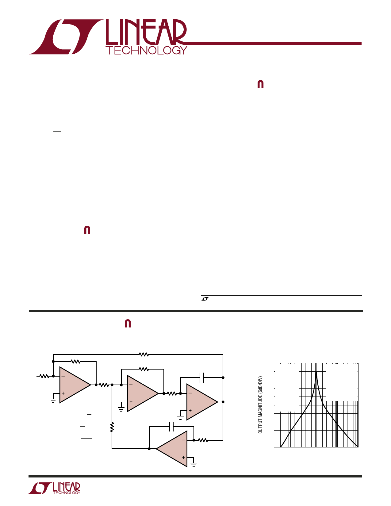
TYPICAL APPLICATIO
Bandpass Filter with Independently Settable Gain, Q and fC
R1
RG
VIN
RQ
–
1/4 LT1814
+
GAIN = R1
RG
Q = R1
RQ
fC
=
1
2πRFC
R
R
R
–
1/4 LT1814
+
C
RF
–
1/4 LT1814
+
C
RF
1/4 LT1814
1814 TA01
BANDPASS
OUT
Filter Frequency Response
R = 499Ω
0 R1 = 499Ω
RF = 475Ω
RQ = 49.9Ω
RG = 499Ω
C = 3.3nF
fC = 100kHz
Q = 10
GAIN = 1
VS = ±5V
VIN = 5VP-P
DISTORTION:
2nd < –76dB
3rd < –90dB
ACROSS FREQ
RANGE
1k
10k
100k
1M
10M
FREQUENCY (Hz)
1814 TA02
18134fa
1
Share Link: 