1814 데이터 시트보기 (PDF) - Linear Technology
부품명
상세내역
제조사
1814 Datasheet PDF : 16 Pages
| |||
LT1813/LT1814
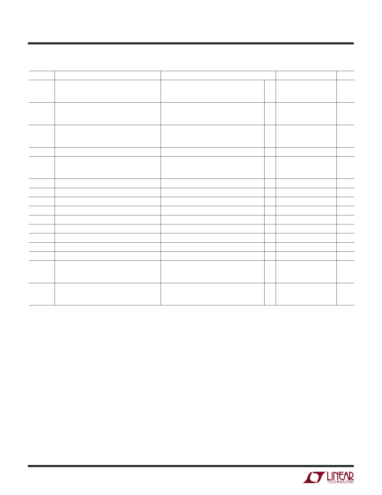
ELECTRICAL CHARACTERISTICS The ● denotes the specifications which apply over the full operating
temperature range, otherwise specifications are at TA = 25°C. VS = 5V, VCM = 2.5V, RL to 2.5V, unless otherwise noted. (Note 8)
SYMBOL PARAMETER
CONDITIONS
MIN TYP MAX UNITS
IOUT
Maximum Output Current
ISC
Output Short-Circuit Current
SR
Slew Rate
FPBW
Full Power Bandwidth
VOUT = 1.5V or 3.5V, 30mV Overdrive
±25 ±35
mA
TA = 0°C to 70°C
● ±20
mA
TA = – 40°C to 85°C
● ±17
mA
VOUT = 2.5V, 1V Overdrive (Note 3)
±55 ±75
mA
TA = 0°C to 70°C
● ±45
mA
TA = – 40°C to 85°C
● ±40
mA
AV = –1 (Note 5)
TA = 0°C to 70°C
TA = – 40°C to 85°C
200
350
V/µs
● 150
V/µs
● 125
V/µs
2VP-P (Note 6)
55
MHz
GBW
Gain Bandwidth Product
–3dB BW
tr, tf
–3dB Bandwidth
Rise Time, Fall Time
f = 200kHz, RL = 500Ω
TA = 0°C to 70°C
TA = – 40°C to 85°C
65
94
MHz
● 55
MHz
● 50
MHz
AV = 1, RL = 500Ω
180
MHz
AV = 1, 10% to 90%, 0.1V, RL = 100Ω
2.1
ns
tPD
Propagation Delay (Note 10)
OS
Overshoot
AV = 1, 50% to 50%, 0.1V, RL = 100Ω
AV = 1, 0.1V, RL = 100Ω
3
ns
25
%
tS
Settling Time
THD
Total Harmonic Distortion
dG
Differential Gain
AV = –1, 0.1%, 2V
AV = 2, f = 1MHz, VOUT = 2VP-P, RL = 500Ω
AV = 2, VOUT = 2VP-P, RL = 150Ω
30
ns
–75
dB
0.22
%
dP
Differential Phase
ROUT
Output Resistance
AV = 2, VOUT = 2VP-P, RL = 150Ω
AV = 1, f = 1MHz
0.21
DEG
0.45
Ω
Channel Separation
IS
Supply Current
VOUT = 1.5V to 3.5V, RL = 100Ω
TA = 0°C to 70°C
TA = – 40°C to 85°C
Per Amplifier
TA = 0°C to 70°C
TA = – 40°C to 85°C
81
100
dB
● 80
dB
● 79
dB
2.9
4.0
mA
●
5.0
mA
●
5.5
mA
Note 1: Absolute Maximum Ratings are those values beyond which the life
of the device may be impaired.
Note 2: Differential inputs of ±6V are appropriate for transient operation
only, such as during slewing. Large sustained differential inputs can cause
excessive power dissipation and may damage the part.
Note 3: A heat sink may be required to keep the junction temperature
below absolute maximum when the output is shorted indefinitely.
Note 4: Input offset voltage is pulse tested and is exclusive of warm-up
drift.
Note 5: Slew rate is measured between ±2V at the output with ±3V input
for ±5V supplies and 2VP-P at the output with a 3VP-P input for single 5V
supplies.
Note 6: Full power bandwidth is calculated from the slew rate:
FPBW = SR/2πVP
Note 7: This parameter is not 100% tested
Note 8: The LT1813C/LT1814C are guaranteed to meet specified
performance from 0°C to 70°C and is designed, characterized and
expected to meet the extended temperature limits, but is not tested at
–40°C and 85°C. The LT1813I/LT1814I are guaranteed to meet the
extended temperature limits.
Note 9: The LT1813D is 100% production tested at 25°C. It is designed,
characterized and expected to meet the 0°C to 70°C specifications
although it is not tested or QA sampled at these temperatures. The
LT1813D is guaranteed functional from –40°C to 85°C but may not meet
those specifications.
Note 10: Propagation delay is measured from the 50% point on the input
waveform to the 50% point on the output waveform.
18134fa
6
Share Link: 