HFCT-5305 데이터 시트보기 (PDF) - HP => Agilent Technologies
부품명
상세내역
제조사
HFCT-5305
HP => Agilent Technologies

HFCT-5305 Datasheet PDF : 8 Pages
| |||
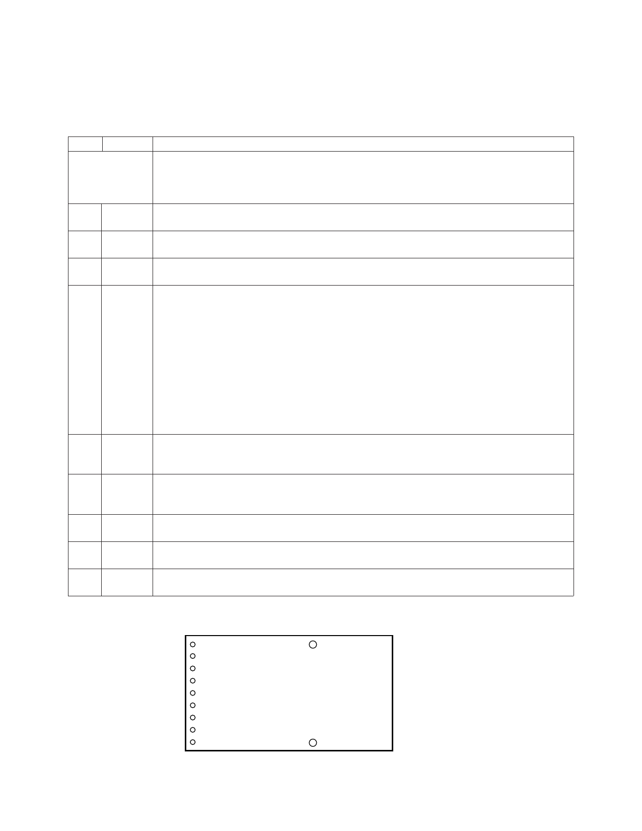
Table 1. Pinout Table
Pin Symbol
Mounting Studs
1
VEER
2
RD+
3
RD–
4
SD
Functional Description
The mounting studs are provided for transceiver mechanical attachment to the circuit
board, they are embedded in the nonconductive plastic housing and are not tied to the
transceiver internal circuit. They should be soldered into plated-through holes on the
printed circuit board.
Receiver Signal Ground
Directly connect this pin to receiver signal ground plane.
Receiver Data Out
See recommended circuit schematic.
Receiver Data Out Bar
See recommended circuit schematic.
Signal Detect
Normal optical input levels to the receiver result in a logic “1” output.
Low optical input levels to the receiver result in a fault condition indication shown by
a logic “0” output.
Signal Detect is a single-ended, low-power, PECL output. Since SD is a low-power
PECL output, complete the interconnection of SD output with other PECL inputs using
a 10 kΩ pull-down resistor to VEE to allow biasing of this interconnection. Do not load
this SD output with standard PECL, 50 Ω to VCC – 2 V, termination. If Signal Detect
output is not used, leave it open-circuited.
This Signal Detect output can be used to drive a PECL input on an upstream circuit,
such as, Signal Detect input or Loss of Signal-bar.
5
VCCR Receiver Power Supply
Provide +5 V dc via the recommended transmitter power supply filter circuit.
Locate the power supply filter circuit as close as possible to the VCCR pin.
6
VCCT Transmitter Power Supply
Provide +5 V dc via the recommended transmitter power supply filter circuit.
Locate the power supply filter circuit as close as possible to the VCCT pin.
7
TD– Transmitter Data In Bar
See recommended circuit schematic.
8
TD+ Transmitter Data In
See recommended circuit schematic.
9
VEET Transmitter Signal Ground
Directly connect this pin to the transmitter signal ground plane.
RECEIVER SIGNAL GROUND
1
RECEIVER DATA OUT
2
RECEIVER DATA OUT BAR
3
SIGNAL DETECT
4
RECEIVER POWER SUPPLY
5
TRANSMITTER POWER SUPPLY
6
TRANSMITTER DATA IN BAR
7
TRANSMITTER DATA IN
8
TRANSMITTER SIGNAL GROUND
9
Figure 1. Pinout.
570
N/C
N/C
TOP VIEW
Share Link: