M52758SP 데이터 시트보기 (PDF) - Vishay Semiconductors
부품명
상세내역
제조사
M52758SP Datasheet PDF : 15 Pages
| |||
M52758SP/FP
Tr1, Tf1, Tr2, Tf2 Pulse Characteristic
1. The condition is as Table. Set SW19 to GND (or OPEN).
2. The rising of 10% to 90% for input pulse is Tri, the falling of 10% to 90% for input pulse is Tfi.
3. Next, the rising of 10% to 90% for output pulse is Tro, the falling of 10% to 90% for output pulse is Tfo.
4. The pulse characteristic Tr1, Tf1 (Tr2, Tf2) is
100%
90%
0%
Tr
Tf
Tr1 (Tr2) = √ (Tro)2 − (Tri)2 (ns)
Tf1 (Tf2) = √ (Tfo)2 − (Tfi)2 (ns)
10%
VOH1, VOH2 High Level Output Voltage
The condition is as Table. Set SW19 to GND (OPEN), input 5 V at input terminal. Measure the output voltage, the
voltage is as VOH1 (VOH2).
VOL1, VOL2 Low Level Output Voltage
The condition is as Table. Set SW19 to GND (OPEN), input 0 V at input terminal. Measure the output voltage, the
voltage is as VOL1 (VOL2).
Vith1, Vith2 Input Selectional Voltage
The condition is as Table. Set SW19 to GND (OPEN), increasing gradually the voltage of input terminal from 0 V,
measure the voltage of input terminal when output terminal is 4.5 V. The input voltage is as Vith1 (Vith2).
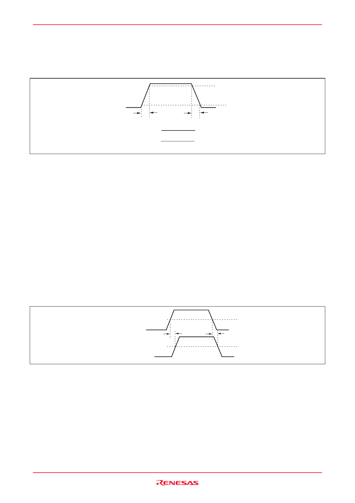
Trd1, Trd2 Rising Delay Time, Tfd1, Tfd2 Falling delay time
The condition is as Table. Set SW19 to GND (OPEN), SG7 is as the input signal of input terminal, measure the
waveform of output.
Rising delay time is as Trd1 (Trd2). Falling delay time is as Tfd1 (Tfd2). Reference to the Figure as shown below.
SG7
Trd
Output waveform
50%
Tfd
50%
Rev.2.00 Sep 14, 2006 page 8 of 14
Share Link: 