M52758SP 데이터 시트보기 (PDF) - Mitsumi
부품명
상세내역
제조사
M52758SP Datasheet PDF : 10 Pages
| |||
MITSUBISHI ICs (Monitor)
M52758SP/FP
WIDE BAND ANALOG SWITCH
5. Measure the crosstalk between channels when SG3 is as the input
signal of Pin 5, Pin 7 .
6. Next, set SW19 to OPEN, SG3 as the input signal of Pin11, measure
the amplitude output from T.P.35. The amplitude is as VOR6.
7.Next, measure the amplitude output from T.P.30, T.P.27 in the same
state. The amplitude is as VOG6, VOB6.
8. The crosstalk between channels C.T.C.2 is
C.T.C2= 20 LOG
VO G 6 or VO B 6 [dB]
VO R6
9. By the same way, measure the crosstalk between channels when
input signal to Pin13, 16.
C.T.C.3,C.T.C.4 Crosstalk between channel
Set SG4 as the input signal, and the same method as Table, measure
C.T.C.3, C.T.C.4.
Tr1,Tf1,Tr2,Tf2 Pulse characteristic
1. The condition is as Table 1. Set SW19 to GND (or OPEN).
2. The rising of 10 % to 90 % for input pulse is Tri, the falling of 10 % to
90 % for input pulse is Tfi.
3. Next, the rising of 10 % to 90 % for output pulse is Tro, the falling of
10 % to 90 % for output pulse is Tfo.
4. The pulse characteristic Tr1, Tf1 ( Tr2, Tf2 ) is
100%
90%
0%
Tr
Tr1(Tr2) =
Tf 1(Tf 2) =
Tf
(Tro)2 - (Tri)2
(Tf o) 2 - (Tf i)2
10%
(nsec)
(nsec)
VOH1,VOH2 High level output voltage
The condition is as Table . Set SW19 to GND (OPEN), input 5V at input
terminal. Measure the output voltage, the voltage is as VOH1 (VOH2).
VOL1,VOL2 Low level output voltage
The condition is as Table . Set SW19 to GND (OPEN), input 0V at input
terminal. Measure the output voltage, the voltage is as VOL1 (VOL2).
Vith1,Vith2 Input selectional voltage
The condition is as Table . Set SW19 to GND (OPEN), increasing
gradually the voltage of input terminal from 0V, measure the voltage of
input terminal when output terminal is 4.5V. The input voltage is as
Vith1(Vith 2).
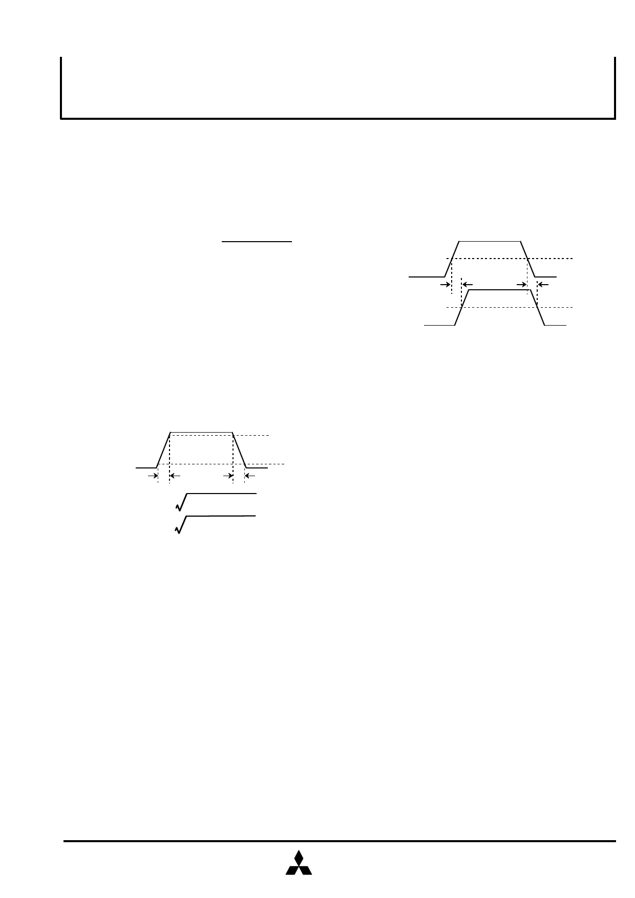
Trd1,Trd2 Rising delay time
Tfd1,Tfd2 Falling delay time
The condition is as Table . Set SW19 to GND (OPEN), SG7 is as
the input signal of input terminal, measure the waveform of output.
Rising delay time is as Trd1 (Trd2). Falling delay time is as
Tfd1(Tfd2). Reference to the Fig. as shown below.
SG7
Trd
Output waveform
50%
Tfd
50%
Vsth1,Vsth2 Switching selectional voltage
1. The condition is as Table . SG1 is as the input signal of Pin2,
Pin5, Pin7, and SG7 is as the input signal of Pin8, Pin9. There is no
input at another pins.
2. Input 0V at Pin19, confirm that there are signals output from
T.P.21, T.P.22, T.P.25, T.P.27,T.P.30,T.P.35.
3. Increase gradually the voltage of terminal Pin19. Read the voltage
when there is no signal output from the terminals listed as above.
The voltage is as Vsth1.
4. SG1 as the input signal of Pin11, Pin13, Pin16, and SG7 as the
input signal of Pin17, Pin18.There is no input at another pins.
5. Inputs 5V at Pin19, confirm that there is no signal output from
T.P.21, T.P.22, T.P.25, T.P.27,T.P.30,T.P.35.
6. Decreasing gradually the voltage of terminal Pin 19. Read the
voltage when there are signals output from the terminals listed as
above. The voltage is as Vsth2.
MITSUBISHI
ELECTRIC
6
Share Link: 