M61503 데이터 시트보기 (PDF) - Renesas Electronics
부품명
상세내역
제조사
M61503 Datasheet PDF : 14 Pages
| |||
M61503FP
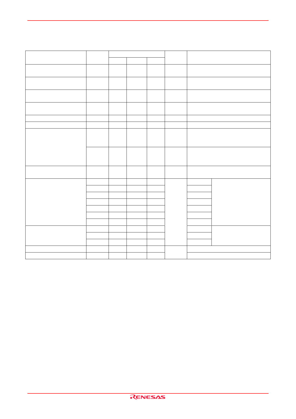
Electrical Characteristics
(VDD = 2.5 V, VSS = −2.5 V, f = 1 kHz, Vi = 100 mV(rms), Vol = 0 dB, Bass = 0 dB, Treble = 0 dB,
Vol/Treble Share AMP = 18 dB, Surround = Bypass, RL = 10 kΩ, Ta = 25°C, unless otherwise noted)
Limits
Item
Symbol Min Typ Max Unit
Conditions
Circuit current of positive
IDD
power supply
—
30
45
mA Quiescent
Circuit current of negative ISS
power supply
—
−30
−45
mA Quiescent
Voltage gain (selector)
Gv1
16
18
20
dB Vol/Treble share amp gain = 18 dB
Bypass
Voltage gain (tone control) Gv2
25.5 27.5 29.5
dB Vol/Treble share amp gain = 18 dB
Q surround mode Vi = 20mVrms
Maximum output voltage
Vomax
1.2
1.6
—
Vrms RL = 10 k, THD = 1%
Total harmonic distortion
THD
—
0.02 0.08
%
BW = 400 to 30 kHz
Output noise voltage
No1
—
8
20 µVrms JIS-A, Rg = 5.1 k,
VOL = the infinitesimal
BYPASS
No2
—
15
40 µVrms JIS-A, Rg = 5.1 k,
VOL = the infinitesimal
BBE3 (High level +11 dB) mode
Maximum attenuation
ATTmax —
−95
−90
dB Output referencelevel (Vo = 1 Vrms),
ATT = the infinitesimal, JIS-A
Bass boost
GB1
1.5
3
4.5
dB 3 dB
f = 1 kHz, Vo = 80 mVrms
GB2
4.5
6
7.5
6 dB
GB3
7.5
9
10.5
9 dB
GB4
10.5
12
13.5
12 dB
GB5
13.5
15
16.5
15 dB
GB6
16.5
18
19.5
18 dB
GB7
19.5
21
22.5
21 dB
Treble boost
GT1
1.5
3
4.5
3 dB
f = 1 kHz, Vo = 80 mVrms
GT2
4.5
6
7.5
6 dB
GT3
7.5
9
10.5
9 dB
Low level boost (f = 20Hz) BBE1
—
3
—
dB f = 20 Hz, Vo = 80 mVrms
High level boost (f = 10kHz) BBE2
—
11
—
f = 10 kHz, Vo = 80 mVrms
REJ03F0214-0201 Rev.2.01 Mar 31, 2008
Page 10 of 13
Share Link: 