M62501FP 데이터 시트보기 (PDF) - Renesas Electronics
부품명
상세내역
제조사
M62501FP Datasheet PDF : 11 Pages
| |||
M62501P/FP
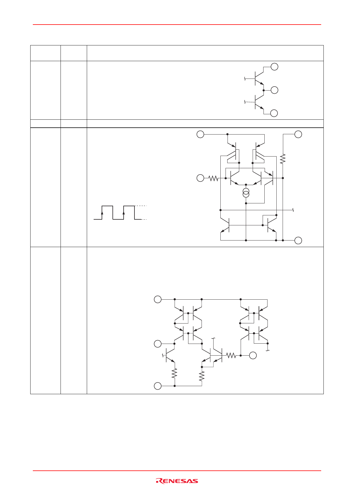
Terminal Functional Description and Equivalent Circuit
Terminal
No.
1
Symbol
PWM
OUT
Function and Terminal Circumscription Circuitry
PWM output terminal
• The PWM output synchronized with the TIN
input.
• Output "H" level = 10.5 V typ
(The output load current: −100 mA, VCC = 12 V)
• Output "L" level = 0.7 V typ
2 VCC
1
PWM
OUT
(The output load current: +100 mA, VCC = 12 V)
16 GND
2
VCC
Power supply terminal
3
TIN
Trigger input terminal
• Frequency range
15 kHz to 150 kHz
• It takes in a start edge.
VCC 2
15 VREF
TIN 3
TIN input waveform
Max 2.5 V
Min 1.0 V
16 GND
4
COSC
Cosc terminal
• It generates a saw wave by connecting capacitor between 4-pin and GND.
• Recommended capacitor value is 1000 pF.
5
CAGC
CAGC terminal
• It sets up sensitivity of AGC by connecting capacitor between 5-pin and GND.
• Recommended capacitor value is 1 µF.
VREF 15
COSC 4
GND 16
5 CAGC
Rev.2.00 Jun 14, 2006 page 4 of 10
Share Link: 