MMJT9410 데이터 시트보기 (PDF) - ON Semiconductor
부품명
상세내역
제조사
MMJT9410 Datasheet PDF : 5 Pages
| |||
MMJT9410
100
10
0.5 ms
1.0
5.0 ms
100 ms
0.1
VCE = 10 V
ftest = 1.0 MHz
TA = 25°C
10
0.1
1.0
10
IC, COLLECTOR CURRENT (AMP)
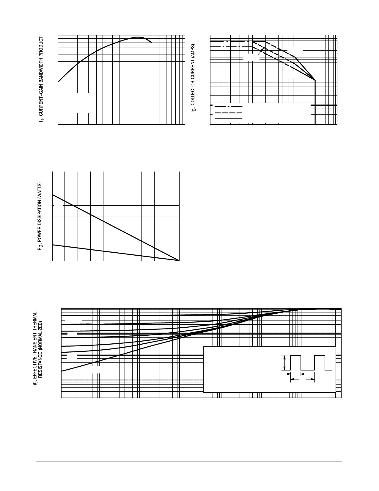
Figure 9. Current−Gain Bandwidth Product
0.01
0.001
0.1
BONDING WIRE LIMIT
THERMAL LIMIT (Single Pulse)
SECONDARY BREAKDOWN LIMIT
1.0
10
100
VCE, COLLECTOR−EMITTER VOLTAGE (VOLTS)
Figure 10. Active Region Safe Operating Area
4.0
3.0
TC
2.0
1.0
TA
0
25
50
75
100
125
T, TEMPERATURE (°C)
Figure 11. Power Derating
There are two limitations on the power handling ability of
a transistor: average junction temperature and secondary
breakdown. Safe operating area curves indicate IC − VCE
limits of the transistor that must be observed for reliable
operation; i.e., the transistor must not be subjected to greater
dissipation than the curves indicate.
The data of Figure 10 is based on TJ(pk) = 150°C; TC is
variable depending on conditions. Secondary breakdown
pulse limits are valid for duty cycles to 10% provided TJ(pk)
v 150°C. TJ(pk) may be calculated from the data in
Figure 12. At high case temperatures, thermal limitations
will reduce the power that can be handled to values less than
150
the limitations imposed by secondary breakdown.
1.0
0.1
0.01
D = 0.5
0.2
0.1
0.05
0.02
0.01
0.001
SINGLE PULSE
0.0001
0.0001
0.001
RqJA(t) = r(t) qJA
qJA = 165°C/W
D CURVES APPLY FOR POWER
PULSE TRAIN SHOWN
READ TIME AT t1
TJ(pk) − TA = P(pk) qJA(t)
P(pk)
t1
t2
DUTY CYCLE, D = t1/t2
0.01
0.1
1.0
10
100
1000
t, TIME (seconds)
Figure 12. Thermal Response
http://onsemi.com
4
Share Link: 