NCS2002 데이터 시트보기 (PDF) - ON Semiconductor
부품명
상세내역
제조사
NCS2002 Datasheet PDF : 16 Pages
| |||
NCS2002, NCV2002
Sub−One Volt Rail−to−Rail
Operational Amplifier with
Enable Feature
The NCS2002 is an industry first sub−one volt operational amplifier
that features a rail−to−rail common mode input voltage range, along
with rail−to−rail output drive capability. This amplifier is guaranteed
to be fully operational down to 0.9 V, providing an ideal solution for
powering applications from a single cell Nickel Cadmium (NiCd) or
Nickel Metal Hydride (NiMH) battery. Additional features include no
output phase reversal with overdriven inputs, trimmed input offset
voltage of 0.5 mV, extremely low input bias current of 40 pA, and a
unity gain bandwidth of 1.1 MHz at 5.0 V.
The NCS2002 also has an active high enable pin that allows external
shutdown of the device. In the standby mode, the supply current is
typically 1.9 mA at 1.0 V. Because of its small size and enable feature,
this amplifier represents the ideal solution for small portable
electronic applications. The NCS2002 is available in the space saving
SOT23−6 (TSOP−6) package with two industry standard pinouts.
Features
• 0.9 V Guaranteed Operation
• Standby Mode: ID = 1.9 mA at 1.0 V, Typical
• Rail−to−Rail Common Mode Input Voltage Range
• Rail−to−Rail Output Drive Capability
• No Output Phase Reversal for Over−Driven Input Signals
• 0.5 mV Trimmed Input Offset
• 10 pA Input Bias Current
• 1.1 MHz Unity Gain Bandwidth at $2.5 V, 1.0 MHz at $0.5 V
• Tiny SOT23−6 (TSOP−6) Package
• Pb−Free Packages are Available
Typical Applications
• Single Cell NiCd / NiMH Battery Powered Applications
• Cellular Telephones
• Pagers
• Personal Digital Assistants
• Electronic Games
• Digital Cameras
• Camcorders
• Hand Held Instruments
Rail to Rail Input
Rail to Rail Output
0.8 V
to
7.0 V
+
−
This device contains 81 active transistors.
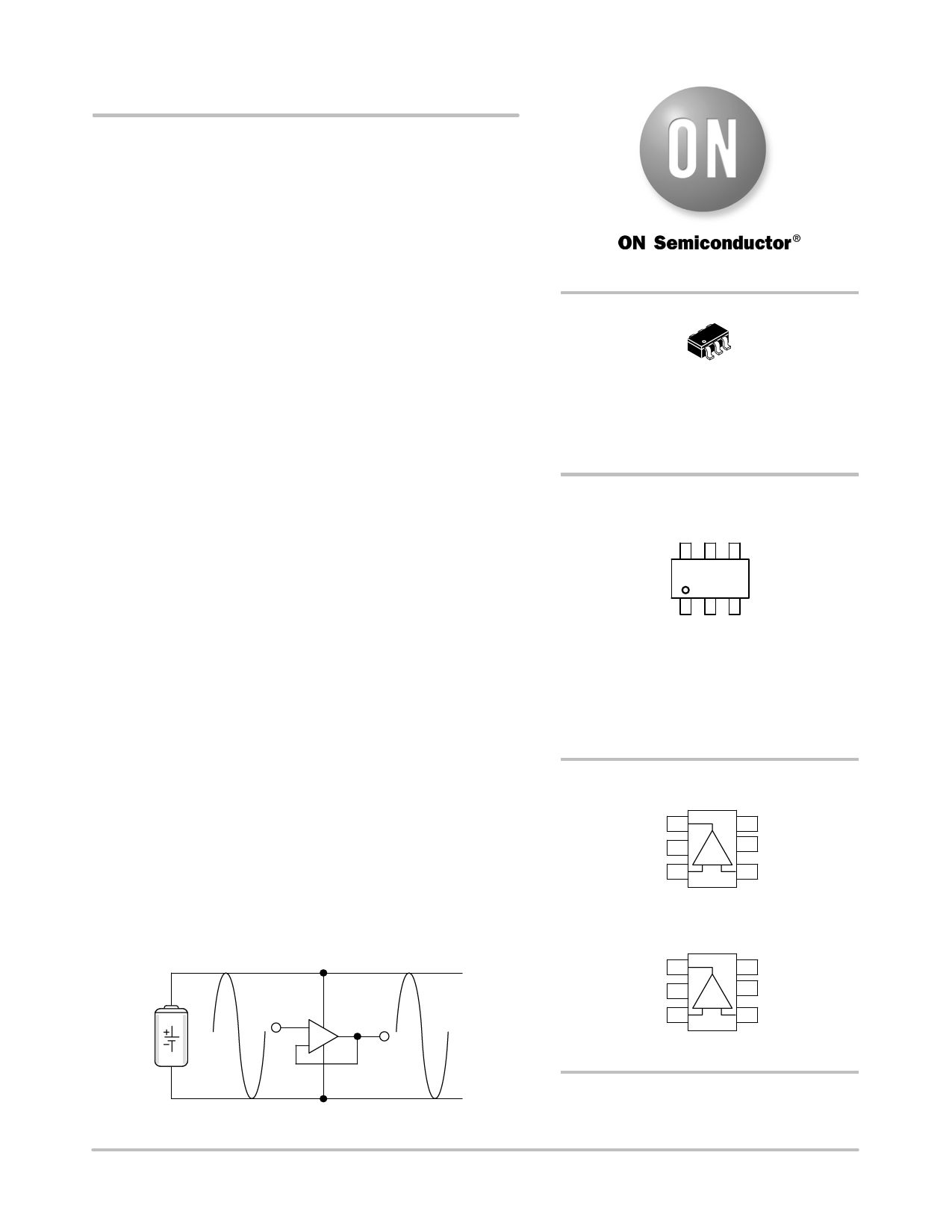
Figure 1. Typical Application
© Semiconductor Components Industries, LLC, 2007
1
January, 2007 − Rev. 6
http://onsemi.com
1
TSSOP−6
SN SUFFIX
CASE 318G
MARKING DIAGRAM
AAxAYW G
G
1
AA = Device Code
x = Marking Defined on Page 15 in
Ordering Information
A = Assembly Location
Y = Year
W = Work Week
G = Pb−Free Package
(Note: Microdot may be in either location)
PIN CONNECTIONS
VOUT 1
6 VEE
VCC 2 + − 5 Enable
Non−Inverting
Input
3
4
Inverting
Input
Style 1 Pinout (SN1T1)
VOUT 1
6 VCC
VEE 2 + − 5 Enable
Non−Inverting
Input
3
4
Inverting
Input
Style 2 Pinout (SN2T1)
ORDERING AND MARKING INFORMATION
See detailed ordering, marking, and shipping information in
the package dimensions section on page 15 of this data sheet.
Publication Order Number:
NCS2002/D
Share Link: 