NCS2002 데이터 시트보기 (PDF) - ON Semiconductor
부품명
상세내역
제조사
NCS2002 Datasheet PDF : 16 Pages
| |||
NCS2002, NCV2002
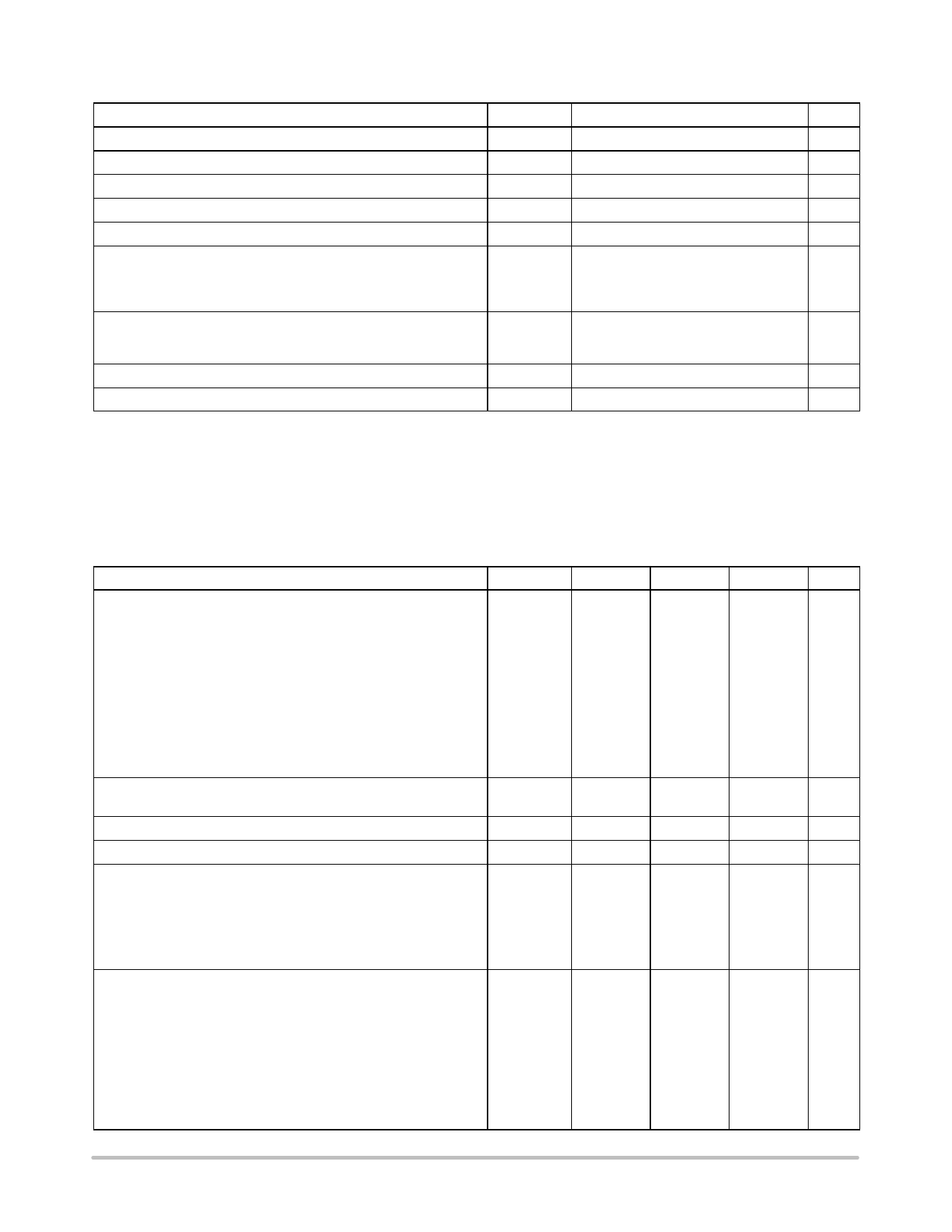
MAXIMUM RATINGS
Rating
Symbol
Value
Unit
Supply Voltage (VCC to VEE)
Input Differential Voltage Range (Note 1)
Input Common Mode Voltage Range (Note 1)
Output Short Circuit Duration (Note 2)
Junction Temperature
Power Dissipation and Thermal Characteristics
SOT23−6 Package
Thermal Resistance, Junction−to−Air
Power Dissipation @ TA = 70°C
Operating Ambient Temperature Range
NCS2002
NCV2002 (Note 3)
VS
VIDR
VICR
tSc
TJ
RqJA
PD
TA
7.0
VEE – 300 mV to 7.0 V
VEE – 300 mV to 7.0 V
Indefinite
150
235
340
−40 to 105
−40 to 125
V
V
V
sec
°C
°C/W
mW
°C
Storage Temperature Range
Tstg
−65 to 150
°C
ESD Protection at any Pin Human Body Model (Note 4)
VESD
2000
V
Stresses exceeding Maximum Ratings may damage the device. Maximum Ratings are stress ratings only. Functional operation above the
Recommended Operating Conditions is not implied. Extended exposure to stresses above the Recommended Operating Conditions may affect
device reliability.
1. Either or both inputs should not exceed the range of VEE – 300 mV to VEE + 7.0 V.
2. Maximum package power dissipation limits must be observed to ensure that the maximum junction temperature is not exceeded.
TJTA + (PD RqJA)
3. NCV prefix is for automotive and other applications requiring site and change control.
4. ESD data available upon request.
DC ELECTRICAL CHARACTERISTICS (VCC = 2.5 V, VEE = −2.5 V, VCM = VO = 0 V, RL to GND, TA = 25°C, unless otherwise noted)
Rating
Symbol
Min
Typ
Max
Unit
Input Offset Voltage
VCC = 0.45 V, VEE = −0.45 V
TA = 25°C
TA = 0°C to 70°C
TA = −40 to +125°C
VCC = 1.5 V, VEE = −1.5 V
TA = 25°C
TA = 0°C to 70°C
TA = −40 to +125°C
VCC = 2.5 V, VEE = −2.5 V
TA = 25°C
TA = 0°C to 70°C
TA = −40 to +125°C
Input Offset Voltage Temperature Coefficient (RS = 50)
TA = −40 to +125°C
VIO
−6.0
0.5
−8.5
−
−9.5
−
−6.0
0.5
−7.0
−
−7.5
−
−6.0
0.5
−7.5
−
−7.5
−
DVIO / DT
−
8.0
mV
6.0
8.5
9.5
6.0
7.0
7.5
6.0
7.5
7.5
−
mV/°C
Input Bias Current (VCC = 1.0 V to 5.0 V)
IIB
−
10
−
pA
Input Common Mode Voltage Range
VICR
−
VEE to VCC
−
V
Large Signal Voltage Gain
VCC = 0.45 V, VEE = −0.45 V
RL = 10 k
VCC = 1.5 V, VEE = −1.5 V
RL = 10 k
VCC = 2.5 V, VEE = −2.5 V
RL = 10 k
AVOL
−
40
−
40
10
40
kV/V
−
−
−
Output Voltage Swing, High State Output (VID = + 0.5 V)
TA = Tlow to Thigh
VCC = 0.45 V, VEE = −0.45 V
RL = 10 k
RL = 2.0 k
VCC = 1.5 V, VEE = −1.5 V
RL = 10 k
RL = 2.0 k
VCC = 2.5 V, VEE = −2.5 V
RL = 10 k
RL = 2.0 k
VOH
V
0.40
0.442
−
0.35
0.409
−
1.45
1.494
−
1.40
1.473
−
2.45
2.493
−
2.40
2.469
−
http://onsemi.com
2
Share Link: 