NX26F011A 데이터 시트보기 (PDF) - Unspecified
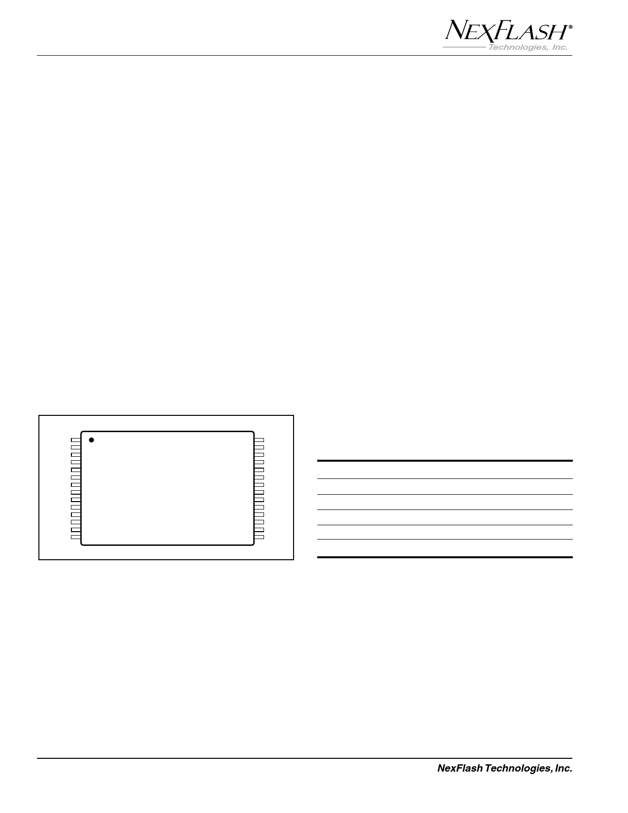
부품명
상세내역
제조사
NX26F011A Datasheet PDF : 14 Pages
| |||
NX26F011A
NX26F041A
Pin Descriptions
Package Types
The NX26F011A and NX26F041A is available in a 24/28-pin
TSOP (Type II) package (Figure 1 and Table 1) or a
removable Serial Flash Module (see NX25Mxxx/NX26Mxxx
Serial Flash Module data sheet for further information).
Power Supply Pins (Vcc and GND)
The NX26F011A and NX26F041A support single power sup-
ply Read, Erase, and Write operations available in 5V and 3V
Vcc versions. Active power requirements are as low as 15 mA
for 3V versions with standby current in the 1 µA range.
NXS Serial Interface Pins (SCK and SIO)
The 2-wire NXS (NexFlash Serial) interface includes a
Clock Input pin (SCK) and a single bidirectional I/O pin for
data (SIO). All data to or from the SIO pin is clocked
relative to the rising edge of SCK. The 2-wire NXS serial
interface makes the NX26F011A and NX26F041A an ideal
solution for removable non-volatile storage. A simple edge
connector or cable/connector with four contacts (SCK,
SIO, Vcc, and GND) can support communications with
space efficiency and reliability. The NXS interface can
operate at clock rates up to 16 MHz for 5V versions.
Device Address Pins (A0, A1, A2, A3)
There is no active chip select on the NX26F011A and
NX26F041A. Instead, four static device address pins
(A0, A1, A2, and A3) are provided for decoding from one to
16 possible devices (Figure 2). This allows up to 4MB (using
an NX26F011A device) or 32MB (using an NX26F041A
device) to be addressed via a single 2-wire NXS interface.
The static address pins (A0-A3) must be tied high or low to
match the device address field (DA3-DA0) in the sector
Read and Erase/Write instruction sequences.
No Connect Pins (N/C)
The NX26F011A and NX26F041A uses only a few signal
pins. As a result, the TSOP package has numerous
no connects (NC) that have no electrical contact to the die.
A0 1
NC 2
A2 3
NC 4
NC 5
VCC 6
GND 7
NC 8
NC 9
NC 10
A3 11
SCK 12
A1 13
SIO 14
28
NC
27
NC
26
NC
25
NC
24
NC
23
NC
22
NC
21
NC
20
NC
19
NC
18
NC
17
NC
16
NC
15
NC
Figure 1. NX26F011A and NX26F041A Pin
Assignments
Table 1. Pin Descriptions
A0, A1, A2, A3
SCK
SIO
Vcc
GND
NC
Device Address
Serial Clock
Serial Data I/O
Power Supply
Ground
No Connect
2
NexFlash Technologies, Inc.
PRELIMINARY NXSF009A-0599
05/05/99 ©
Share Link: 