PA15 데이터 시트보기 (PDF) - Apex Microtechnology
부품명
상세내역
제조사
PA15 Datasheet PDF : 4 Pages
| |||
PA15 • PA15A
OPERATING
CONSIDERATIONS
GENERAL
Please read Application Note 1 “General Operating Consid-
erations”, which covers stability, supplies, heatsinking, mount-
ing, current limit, SOA interpretation, and specification inter-
pretation. Additional information can be found in other applica-
tion notes. For information on the package outline, heatsinks,
and mounting hardware, consult the “Accessory and Package
Mechanical Data” section of the data book.
CURRENT LIMIT
For proper operation, the current limit resistor (RCL) must be
connected as shown in the external connection diagram. The
minimum value is 2 ohm, however for optimum reliability the
resistor value should be set as high as possible. The value is
calculated as follows; with the maximum practical value of 150
ohms.
.6
RCL =
ILIM
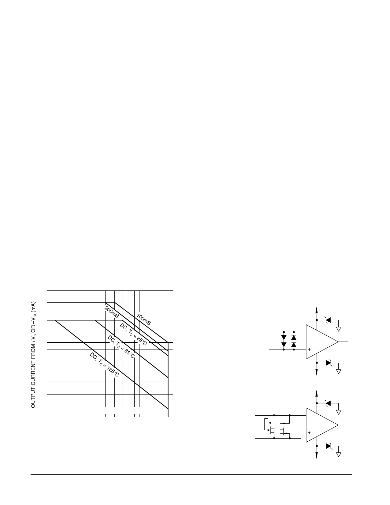
SAFE OPERATING AREA (SOA)
The MOSFET output stage of this power operational ampli-
fier has two distinct limitations:
1. The current handling capability of the MOSFET geometry
and the wire bonds.
2. The junction temperature of the output MOSFETs.
NOTE: The output stage is protected against transient flyback.
However, for protection against sustained, high energy flyback,
external fast-recovery diodes should be used. Pulsed output
currents may not reach 350 mA with VS – VO less than 25V.
500
300
200
200mS
DC, T
100mS
100
DC, T
C = 25°C
DC, T
C = 85°C
50
C = 125°C
30
20
PULSE CURVES @ 10% DUTY CYCLE MAX
10
25
50 75 100 125
250
500
SUPPLY TO OUTPUT DIFFERENTIAL, VS –VO (V)
INPUT PROTECTION
Although the PA15 can withstand differential input voltages
up to ±25V, additional external protection is recommended. In
most applications 1N4148 or 1N914 signal diodes are suffi-
cient (D1-D4 in Figure 2a). In more demanding applications
where low leakage or low capacitance are of concern 2N4416
or 2N5457-2N5459 JFETs connected as diodes will be re-
quired (Q1-Q4 in Figure 2b). In either case the input differential
voltage will be clamped to ±1.4V. This is sufficient overdrive to
produce maximum power bandwidth.
POWER SUPPLY PROTECTION
Unidirectional zener diode transient suppressors are recom-
mended as protection on the supply pins. The zeners clamp
transients to voltages within the power supply rating and also
clamp power supply reversals to ground. Whether the zeners
are used or not, the system power supply should be evaluated
for transient performance including power-on overshoot and
power-off polarity reversals as well as line regulation.
Conditions which can cause open circuits or polarity rever-
sals on either power supply rail should be avoided or protected
against. Reversals or opens on the negative supply rail are
known to induce input stage failure. Unidirectional transzorbs
prevent this, and it is desirable that they be both electrically and
physically as close to the amplifier as possible.
STABILITY
The PA15 has sufficient phase margin to be stable with most
capacitive loads at a gain of 10 or more, using the recom-
mended phase compensation.
The PA15 is externally compensated and performance can
be tailored to the ap-
plication. Use the a.
+VS
graphs of small sig-
Z1
nal response and
power response as a
guide. The compen-
sation capacitor CC
must be rated at
500V working volt-
age. An NPO capaci-
–IN
D1
D3
+IN
1
6
D2
PA15
D4
2
5
tor is recommended.
The compensation
Z2
network CCRC must
–VS
be mounted closely b.
to the amplifier pins
+VS
8 and 9 to avoid spu-
Z1
rious oscillation.
–IN
Q1
1
Q2
6
PA15
Q3
+IN
Q4 2
5
FIGURE 2. OVERVOLTAGE PROTECTION
Z2
–VS
This data sheet has been carefully checked and is believed to be reliable, however, no responsibility is assumed for possible inaccuracies or omissions. All specifications are subject to change without notice.
PA15U REV. D MARCH 1999 © 1999 Apex Microtechnology Corp.
Share Link: 