SE1050W 데이터 시트보기 (PDF) - SiGe Semiconductor, Inc.
부품명
상세내역
제조사
SE1050W Datasheet PDF : 11 Pages
| |||
SE1050W
LightCharger™ 10 Gb/s Transimpedance Amplifier
Final
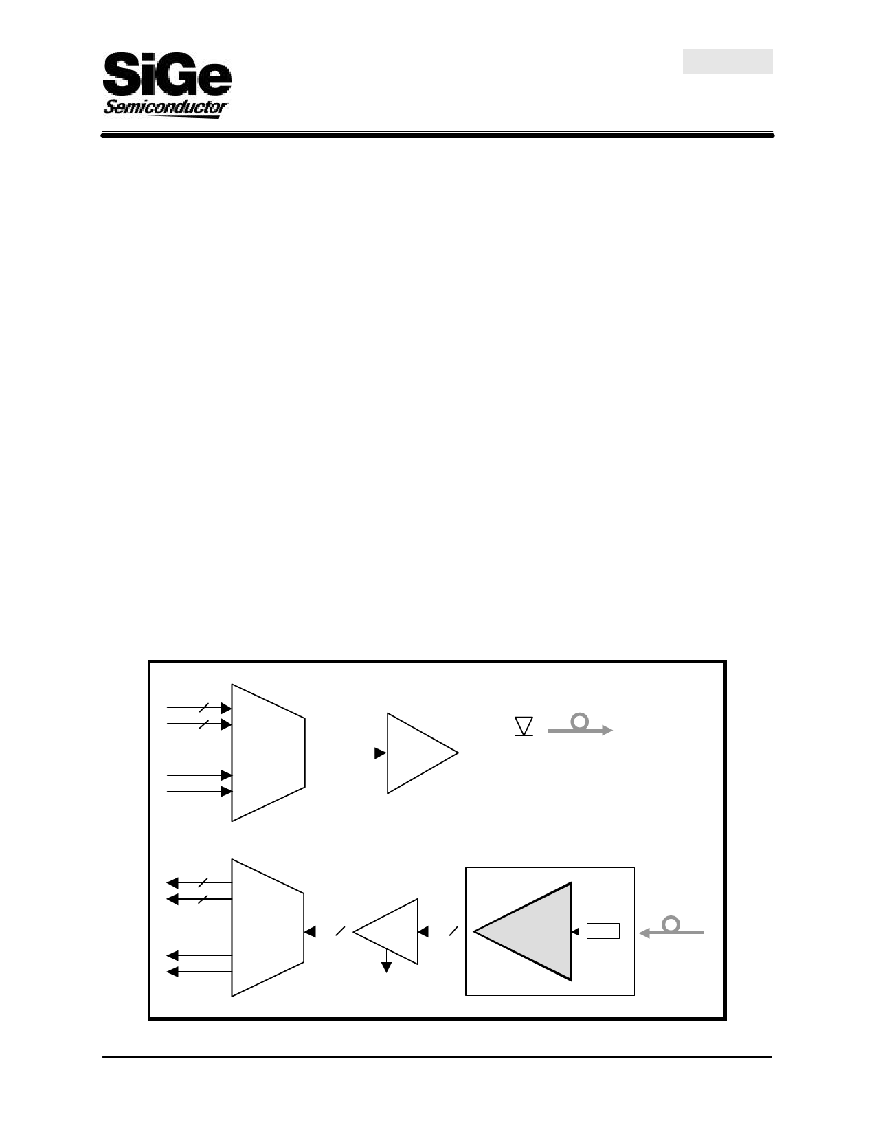
Functional Description
Amplifier Front-End
The transimpedance front-end amplifies the current
from a PIN photodetector, anode connected to pad
TZ_IN, to produce a differential output voltage with
the feedback resistor Rf determining the level of
amplification (see the functional block diagram on
page 1).
The input pad TZ_IN is biased at nominally 1.29 V
above ground, allowing the photodetector to have a
wide reverse-bias by connecting the cathode to VCC.
This enables single rail operation and normally
ensures that the PIN operates in its constant, low-
capacitance region.
The output stage has its own supply connection
VCC2 (+5 V) to maintain integrity of the high-speed
signal path. The output stage shares the GND (0 V)
connection with the remainder of the circuitry, which
has a separate supply connection VCC1 (+5 V).
Output Driver Stage
The output driver acts as a buffer stage, capable of
swinging up to 1.1 V pk-pk differential into a 100 Ω
load.
System Block Diagram
The output can be configured in a differential or
single-ended mode. For differential operation, the pad
ACGND is not wire bonded and the circuit provides a
fully balanced 100 Ω output, on the pins OUTP and
OUTN. For single-ended operation, the ACGND pad
is required to be wire bonded to an external capacitor
to ground (recommend 1 nF). Under these
circumstances, OUTP operates as a single-ended
50 Ω output. In both cases, increasing optical input
level gives a positive-going output signal on the
OUTP pin.
Power Supply Rejection
An on-chip power supply rejection circuit is used to
achieve both single-ended and differential rejection
from the +5 V VCC rail. This rejection ensures that
performance is not degraded by noise on the power
supply. The circuit achieves a power supply rejection
on the outputs of 38 dB for single-ended and 24 dB
for differential operation, up to 100 kHz. The use of
external decoupling will help to remove any unwanted
signals at higher frequencies.
Data
Mux
Ck In
Data
CDR &
Demux
Clock
Laser
Driver
SE1150/51/52
SE1250
Receiver Module
2
Post
2
Amplifier
SE1050W
PIN
TZ
LOS
Amplifier
45-DST-01 § Rev 1.5 § May 24/02
3 of 11
Share Link: 