SLVU2.8 데이터 시트보기 (PDF) - Weitron Technology
부품명
상세내역
제조사
SLVU2.8 Datasheet PDF : 7 Pages
| |||
SLVU2.8
Application Note
The SLVU2.8 is ideal for providing protection for electronic equipment that is susceptible to damage
caused by Electrostatic Discharge (ESD), Electrical Fast Transients (EFT) and tertiary lightning effects.
This product is offered in a unidirectional configuration and provides both commonmode or
differential-mode protection.
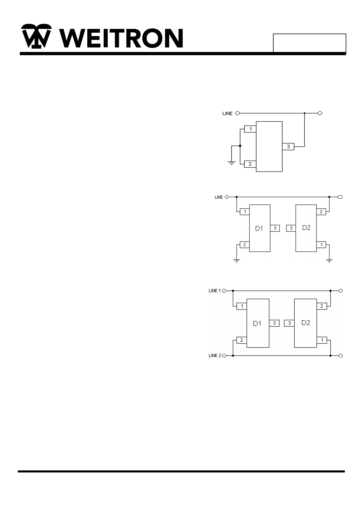
Unidirectional Common-Mode Protection (Fig.9)
The SLVU2.8 provides one line of unidirectional protection
in a common-mode configuration as depicted in figure 9.
Circuit connectivity is as follows:
Line 1 is connected to Pin 3
Pins 1 and 2 are connected to ground
Bidirectional Common-Mode Protection (Fig.10)
Two SLVU2.8 devices provide one line of bidirectional
protection in a common-mode configuration as depicted
in fig.10
Circuit connectivity is as follows:
* Line 1 is connected to Pin1 of Device 1 & Pin 2 of Device 2
* Pin 2 of Device 1 and Pin 1 of Device 2 are connected to ground
* Pin 3 of both devices is not connected
Fig.9
Fig.10
Bidirectional Differential-Mode Protection (Fig.11)
Two SLVU2.8 devices provide up to two lines of
bidrectional protection in a differenitalmode configuration
as depicted in fig.11
Circuit connectivity is as follows:
* Line 1 is connected to Pin1 of Device 1 & Pin 2 of Device 2
* Line 2 is connected to Pin 2 of Device 1 & Pin 1 of Device 2
Fig.11
Circuit Board Layout Protection
Circuit board layout is critical for Electromagnetic Compatibility (EMC) protection. The following
guidelines are recommended:
* The protection device should be placed near the input terminals or connectors, the device will divert
the transient current immediately before it can be coupled into the nearby traces.
* The path length between the TVS device and the protected line should be minimized.
* All conductive loops including power and ground loops should be minimized.
* The transient current return path to ground should be kept as short as possible to reduce
parasitic inductance.
* Ground planes should be used whenever possible. For multilayer PCBs, use ground vias.
WEITRON
5/7
http://www.weitron.com.tw
19-Apr-07
Share Link: 