SP8854E 데이터 시트보기 (PDF) - Zarlink Semiconductor Inc
부품명
상세내역
제조사
SP8854E Datasheet PDF : 14 Pages
| |||
Preliminary Information SP8854E
296
296
VCC
296
24, 25 FPD, FREF
OUTPUTS
3·3mA
0V
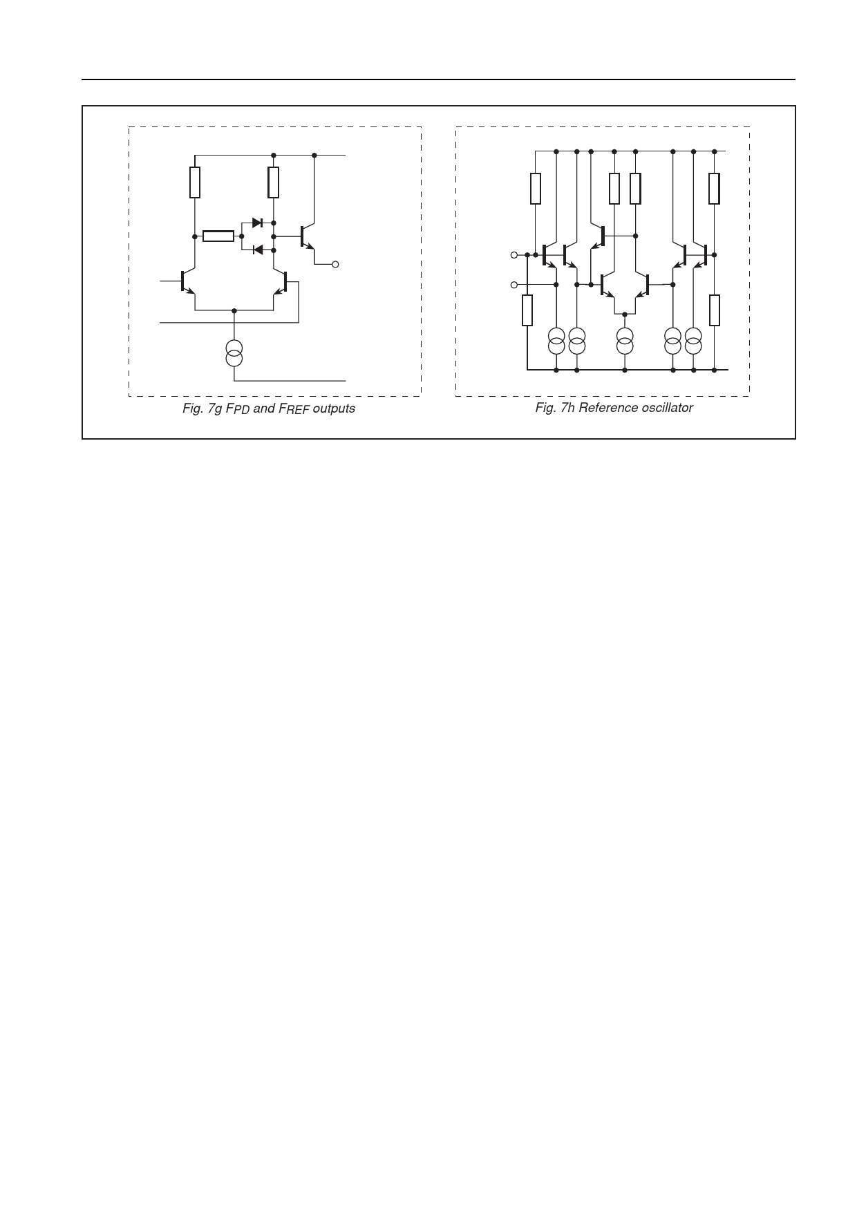
Fig. 7g FPD and FREF outputs
VCC
40k
3k
3k
40k
28
CRYSTAL
27
CAPACITOR
60k
60k
50µA
50µA
100µA
100µA
0V
100µA
Fig. 7h Reference oscillator
Figure 7 - Interface circuit diagrams (continued)
Applications
RF Layout
The SP8854E can operate with input frequencies up to
2·7GHz but to obtain optimum performance, good RF layout
practices should be used. A suitable layout technique is to
use double sided printed circuit board with through plated
holes. Wherever possible the top surface on which the
SP8854E is mounted should be left as a continuous sheet of
copper to form a low impedance ground plane. The ground
pins 12 and 16 should be connected directly to the ground
plane.
Pins such as VCC and the unused RF input should be
decoupled with chip capacitors mounted as close to the
device pin as possible, with a direct connection to the ground
plane; suitable values are 10nF for the power supplies and
<1nF for the RF input pin (a lower value should be used
sufficient to give good decoupling at the RF frequency of
operation). A larger decoupling capacitor mounted as close
as possible to pin 26 should be used to prevent modulation
of VCC by the charge pump pulses. The RSET resistor should
also be mounted close to the RSET pin to prevent noise
pickup. The capacitor connected from the charge pump
output should be a chip component with short connections to
the SP8852E. All signals such as the programming inputs,
RF IN, REFERENCE IN and the connections to the op-amp
are best taken through the pc board adjacent to the SP8852D
with through plated holes allowing connections to remote
points without fragmenting the ground plane.
Programming Bus
The input pins are designed to be compatible with TTL or
CMOS logic with a switching threshold set at about 2·4V by
three forward biased base-emitter diodes. The inputs will be
taken high by an internal pull up resistor if left open circuit but
for best noise immunity it is better to connect unused inputs
directly to VCC or ground.
RF Inputs
The prescaler has a differential input amplifier to improve
input sensitivity. Generally the input drive will be single
ended and the RF signal should be AC coupled to either of
the inputs using a chip capacitor.The remaining input should
be decoupled to ground, again using a chip capacitor. The
inputs can be driven differentially but the input circuit should
not provide a DC path between inputs or to ground.
Lock Detect Circuit
The lock detect circuit uses the up and down correction
pulses from the phase detector to determine whether the
loop is in or out of lock. When the loop is locked, both up and
down pulses are very narrow compared to the reference
frequency, but the pulse width in the out of lock condition
continuously varies, depending on the phase difference
between the outputs of the reference and RF counters. The
logical AND of the up and down pulses is used to switch a
20mA current sink to pin 18 and a 50kΩ resistor provides a
load to VCC. The circuit is shown in Fig. 7c.
When lock is established, the narrow pulses from the
phase detector ensure that the current source is off for the
majority of the time and so pin 18 will be pulled high by the
50kΩ resistor. A voltage comparator with a switching threshold
at about 4·7V monitors the voltage at pin 18 and switches pin
17 low when pin 18 is more positive than the 4·7V threshold.
When the loop is unlocked, the frequency difference at
the counter outputs will produce a cyclic change in pulse
width from the phase detector outputs with a frequency
equal to the difference at the reference and RF counter
outputs. A small capacitor connected to pin 18 prevents the
indication of false phase lock conditions at pin 17 for
momentary phase coincidence. Because of the variable
width pulse nature of the signal at pin 18 the calculation of a
suitable capacitor value is complex, but if an indication with
a delay amounting to several times the expected lock up time
is acceptable, the delay will be approximately equal to the
time constant of the capacitor on pin 18 and the internal
50kΩ resistor. If a faster indication is required, comparable
with the loop lock up time, the capacitor will need to be 2 to
3 times smaller than the time constant calculation suggests.
The time to respond to an out of lock condition is 2 to 3 times
less than that required to indicate lock.
Charge Pump Circuit
The charge pump circuit converts the variable width up
and down pulses from the phase detector into adjustable
current pulses which can be directly connected to the loop
amplifier. The magnitude of the current and therefore the
phase detector gain can be modified when new frequency
data is entered to compensate for change in the VCO gain
characteristic over
9
Share Link: 