TC14433 데이터 시트보기 (PDF) - TelCom Semiconductor Inc => Microchip
부품명
상세내역
제조사
TC14433 Datasheet PDF : 10 Pages
| |||
3-1/2 DIGIT A/D CONVERTERS
1
TC14433
TC14433A
PIN DESCRIPTIONS (Cont.)
Pin No. Pin No. Pin No.
24-Pin 24-Pin 28-Pin
2
PDIP/CerDip SOIC PLCC Symbol Description
16
16
19
DS4 Digit select pins — The digit select output goes high when the respective digit
is selected. The MSD (1/2 digit) turns on immediately after an EOC pulse.
17
17
20
DS3 The remaining digits turn on in sequence from MSD to LSD.
18
18
21
DS2 To ensure that the BCD data has settled, an inter-digit blanking time of two
19
19
23
clock periods is included.
DS1 Clock frequency divided by 80 equals multiplex rate. For example, a system
3
clock of 60 kHz gives a multiplex rate of 0.8 kHz.
20
20
24
Q0
See Figure 12 for digit select timing diagram.
21
21
25
Q1
BCD data output pins — Multiplexed BCD outputs contain three full digits of
information during digit select DS2, DS3, DS4.
22
22
26
Q2
During DS1, the 1/2 digit, overrange, underrange and polarity information is
available.
4
23
23
28
Q3
Refer to truth table.
24
24
28
VDD Positive power supply — This is the most positive power supply pin.
8,15, 22
NC
Not Used.
CIRCUIT DESCRIPTION
The TC14433 CMOS IC becomes a modified dual-
slope A/D with a minimum of external components. This IC
has the customary CMOS digital logic circuitry, as well as
CMOS analog circuitry. It provides the user with digital
functions (such as counters, latches, multiplexers) and
analog functions (such as operational amplifiers and com-
parators) on a single chip.
Features of this system include auto-zero, high input
impedances and auto-polarity. Low power consumption
and a wide range of power supply voltages are also advan-
tages of this CMOS device. The system's auto-zero function
compensates for the offset voltage of the internal amplifiers
and comparators. In this "ratiometric system," the output
reading is the ratio of the unknown voltage to the reference
voltage, where a ratio of 1 is equal to the maximum count of
1999. It takes approximately 16,000 clock periods to com-
plete one conversion cycle. Each conversion cycle may be
divided into 6 segments. Figure 7 shows the conversion
cycle in 6 segments for both positive and negative inputs.
Segment 1 — The offset capacitor (CO), which com-
pensates for the input offset voltages of the buffer and
integrator amplifiers, is charged during this period. How-
ever, the integrator capacitor is shorted. This segment
requires 4000 clock periods.
Segment 2 — During this segment, the integrator
output decreases to the comparator threshold voltage. At
this time, a number of counts equivalent to the input offset
TELCOM SEMICONDUCTOR, INC.
voltage of the comparator is stored in the offset latches for
5 later use in the auto-zero process. The time for this segment
is variable and less than 800 clock periods.
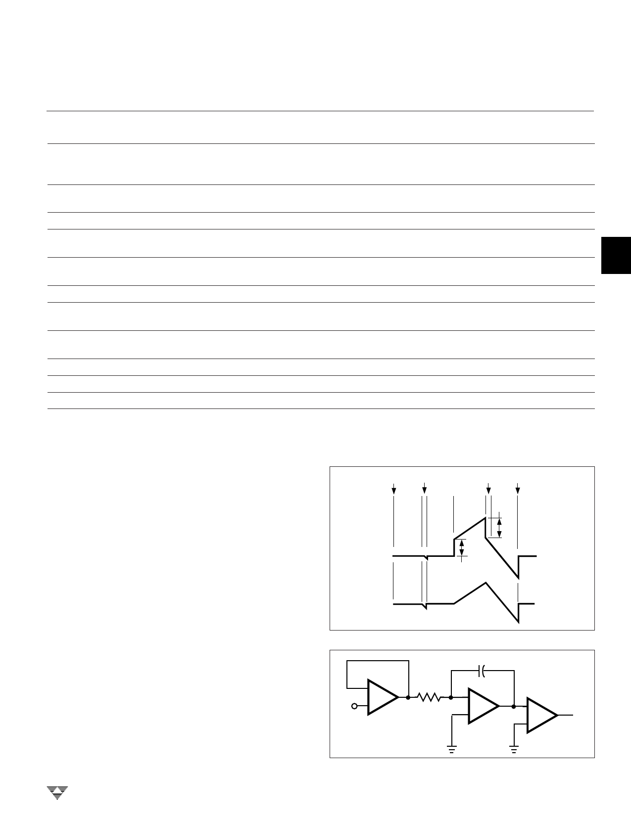
START
TIME
SEGMENT
NUMBER
12 3
END
456
VX
TYPICAL
POSITIVE
INPUT
VOLTAGE
VX
TYPICAL
NEGATIVE
INPUT
VOLTAGE
6
Figure 7. Integrator Waveforms at Pin 6
BUFFER
–
VX
+
C1
R1
INTEGRATOR
COMPARATOR
–
+
+
–
7
Figure 8. Equivalent Circuit Diagrams of the Analog
Section During Segment 4 of the Timing Cycle
3-131
8
Share Link: 