TCL1117 데이터 시트보기 (PDF) - TelCom Semiconductor Inc => Microchip
부품명
상세내역
제조사
TCL1117
TelCom Semiconductor Inc => Microchip

TCL1117 Datasheet PDF : 9 Pages
| |||
PRELIMINARY INFORMATION
TCL1117
TCL1117-2.85
TCL1117-3.30
TCL1117-5.00
800mA LOW DROPOUT POSITIVE REGULATORS
ADJUSTABLE AND FIXED 2.85V, 3.30V, 5.00V
ABSOLUTE MAXIMUM RATINGS*
Input Voltage
Operating Voltage:
TCL1117, TCL1117-3.30, TCL1117-5.00 ...... 15V
TCL1117-2.85 ................................................10V
Surge Voltage:
TCL1117, TCL1117-3.30, TCL1117-5.00 ...... 20V
Operating Junction Temperature ............... 0°C to +125°C
Storage Temperature ............................ – 65°C to +150°C
Lead Temperature (Soldering 10 sec) .................... 300°C
*Stresses beyond those listed under "Absolute Maximum Ratings" may
cause permanent damage to the device. These are stress ratings only, and
functional operation of the device at these or any other conditions beyond
those indicated in the operational sections of the specifications is not
implied. Exposure to absolute maximum rating conditions for extended
periods may affect device reliability.
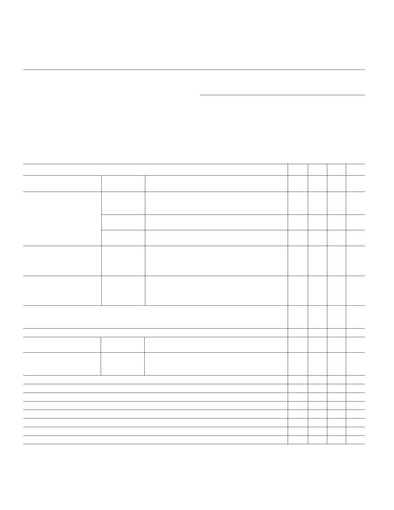
ELECTRICAL CHARACTERISTICS
Symbol Parameter
Test Conditions
Min Typ Max Unit
Reference
Voltage
Output Voltage
TCL1117
TCL1117-2.85
TCL1117-3.30
TCL1117-5.00
Line Regulation
Load Regulation
Dropout Voltage
TCL1117
TCL1117-2.85
TCL1117-3.30
TCL1117-5.00
TCL1117
TCL1117-2.85
TCL1117-3.30
TCL1117-5.00
Current Limit
Minimum Load TCL1117
Current
Quiescent
Current
TCL1117-2.85
TCL1117-3.30
TCL1117-5.00
Thermal Regulation
Ripple Rejection
Adjust Pin Current
Adjust Pin Current Change
Temperature Stability
Long Term Stability
RMS Output Noise
Thermal Resistance
IOUT = 10mA, (VIN – VOUT) = 2V, TJ = 25°C
1.238 1.250 1.262 V
10 ≤ IOUT ≤ 800mA, 1.4V ≤ (VIN – VOUT) ≤ 10V (Note 1) 1.225 1.250 1.270
IOUT = 10mA, VIN = 4.85V, TJ = 25°C
0 ≤ IOUT ≤ 800mA, 4.25V ≤ VIN ≤ 10V (Note 1)
0 ≤ IOUT ≤ 500mA, VIN = 3.95V (Note 1)
2.820 2.850 2.880 V
2.790 2.850 2.910
2.790 2.850 2.910
IOUT = 10mA, VIN = 5.3V, TJ = 25°C
0 ≤ IOUT ≤ 800mA, 4.75V ≤ VIN ≤ 10V (Note 1)
3.265 3.300 3.335 V
3.230 3.300 3.370
IOUT = 10mA, VIN = 7V, TJ = 25°C
0 ≤ IOUT ≤ 800mA, 6.50V ≤ VIN ≤ 12V (Note 1)
4.950 5.000 5.050 V
4.900 5.000 5.100
IOUT = 10mA, 1.5V ≤ VIN – VOUT ≤ 15V (Notes 1 & 2)
IOUT = 0mA, 4.25V ≤ VIN ≤ 10V (Notes 1 & 2)
IOUT = 0mA, 4.75V ≤ VIN ≤ 15V (Notes 1 & 2)
IOUT = 0mA, 6.5V ≤ VIN ≤ 15V (Notes 1 & 2)
— 0.035 0.2 %
—1
6 mV
—1
7
— 1 10
(VIN – VOUT) = 3V, 10mA, ≤ IOUT ≤ 800mA (Notes 1 & 2) — 0.1 0.4 %
VIN = 4.25V, 0 ≤ IOUT ≤ 800mA (Notes 1 & 2)
— 1 10 mV
VIN = 4.75V, 0 ≤ IOUT ≤ 800mA (Notes 1 & 2)
— 1 12
VIN = 6.5V, 0 ≤ IOUT ≤ 800mA (Notes 1 & 2)
— 1 15
IOUT = 100mA, (Note 1 & 3)
IOUT = 500mA, (Note 1 & 3)
IOUT = 800mA, (Note 1 & 3)
— 1.00 1.10 V
— 1.05 1.15
— 1.10 1.20
(VIN – VOUT) = 5V, TJ = 25°C
800 950 1200 mA
(VIN – VOUT) = 15V (Note 1 & 4)
— 1.7 5 mA
VIN ≤ 10V (Note 1)
VIN ≤ 15V (Note 1)
VIN ≤ 15V (Note 1)
TA = 25°C, 30msec Pulse
fRIPPLE = 120Hz (VIN – VOUT) = 3V, VRIPPLE = 1Vp-p ( Note 1)
(Note 1)
10mA ≤ IOUT ≤ 800mA, 1.4V ≤ (VIN – VOUT) ≤ 10V (Note 1)
TA = 125°C, 1000 Hrs.
(% of VOUT), 10Hz ≤ f ≤ 10kHz
(Junction to Case, at Tab)
— 5 10 mA
— 5 10
— 5 10
— 0.01 0.1 %W
60 75 — dB
— 55 120 µA
— 0.2 5 µA
— 0.5 — %
— 0.3 — %
— 0.003 — %
— 15 — °C/W
NOTES: 1. Specifications apply over the full operating temperature range.
2. See thermal regulation specification for changes in output voltage due to heating effects. Load regulation and line regulation are
measured at a constant junction temperature by low duty cycle pulse testing.
3. Dropout voltage is specified over the full output current range of the device. Dropout voltage is defined as the minimum input/output
differential measured at the specified output current. Test points and limits are also shown on the Dropout Voltage curve.
4. Minimum load current is defined as the minimum output current required to maintain regulation.
TCL1117-05 6/5/97
2
Share Link: