TDA1517ATW 데이터 시트보기 (PDF) - NXP Semiconductors.
부품명
상세내역
제조사
TDA1517ATW Datasheet PDF : 19 Pages
| |||
NXP Semiconductors
8 W BTL or 2 × 4 W SE power amplifier
Product specification
TDA1517ATW
handbook, full pagewidth
μc1
MICRO-
CONTROLLER
μc2
μc1 μc2
On
00
Mute 0 1
Standby 1 0
220 nF
IN1+
220 nF
IN2−
VCC
10 kΩ
TDA1517ATW
3
Ri
60 kΩ
18
Ri
60 kΩ
15
16
A
B
VCC
100
1000
nF
μF
8
1000 μF
9
+OUT
RL
4Ω
12
1000 μF
13
−OUT
RL
4Ω
MODE 17
STANDBY/
MUTE LOGIC
8.2
kΩ
5 15 kΩ
VCC
SHORT CIRCUIT
AND
TEMPERATURE
PROTECTION
100
μF
15 kΩ
input
reference
voltage
4
10 11
SGND
PGND
MGU305
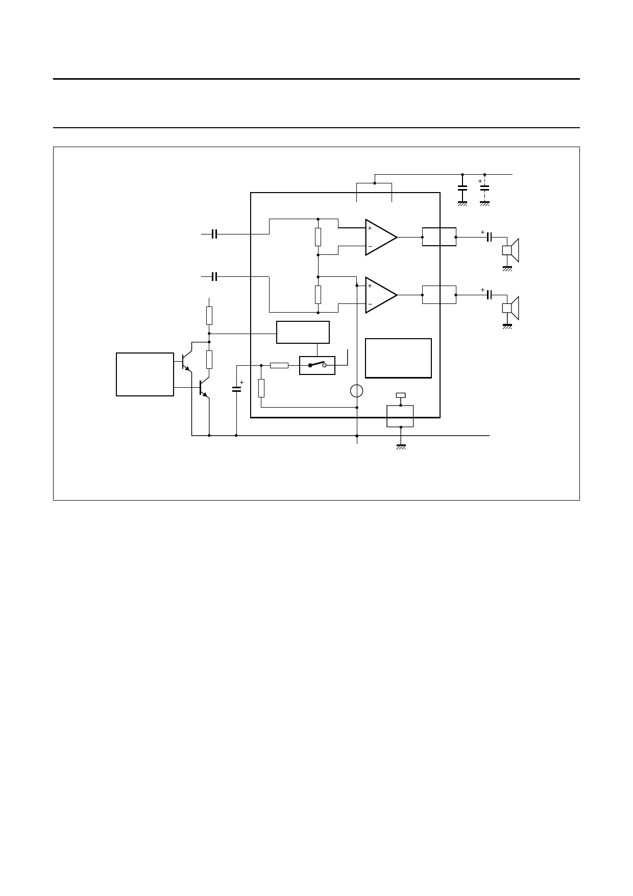
Fig.4 SE application block diagram.
Test conditions
Tamb = 25 °C; unless otherwise specified: VP = 12 V, BTL
application, f = 1 kHz, RL = 8 Ω, fixed gain = 26 dB, audio
band-pass: 22 Hz to 22 kHz. In the figures as a function of
frequency a band-pass of 10 Hz to 80 kHz was applied.
The BTL application block diagram is shown in Fig.3. The
PCB layout [which accommodates both the mono (BTL)
and stereo (single-ended) application] is shown in Fig.6.
Printed-Circuit Board (PCB) layout and grounding
For high system performance levels certain grounding
techniques are imperative. The input reference grounds
have to be tied to their respective source grounds and
must have separate traces from the power ground traces;
this will separate the large (output) signal currents from
interfering with the small AC input signals. The small signal
ground traces should be located physically as far as
possible from the power ground traces. Supply and output
traces should be as wide as possible for delivering
maximum output power.
Proper supply bypassing is critical for low noise
performance and high power supply rejection. The
respective capacitor locations should be as close as
possible to the device and grounded to the power ground.
Decoupling the power supply also prevents unwanted
oscillations. For suppressing higher frequency transients
(spikes) on the supply line a capacitor with low ESR
(typical 0.1 μF) has to be placed as close as possible to the
device. For suppressing lower frequency noise and ripple
signals, a large electrolytic capacitor (e.g. 1000 μF or
greater) must be placed close to the IC.
In single-ended (stereo) application a bypass capacitor
connected to pin SVR reduces the noise and ripple on the
midrail voltage. For good THD and noise performance a
low ESR capacitor is recommended.
Input configuration
It should be noted that the DC level of the input pins is
approximately 2.1 V; a coupling capacitor is therefore
necessary.
2001 Apr 17
8
Share Link: 