TDA4857 데이터 시트보기 (PDF) - Philips Electronics
부품명
상세내역
제조사
TDA4857 Datasheet PDF : 56 Pages
| |||
Philips Semiconductors
I2C-bus autosync deflection controller for
PC monitors
Product specification
TDA4857PS
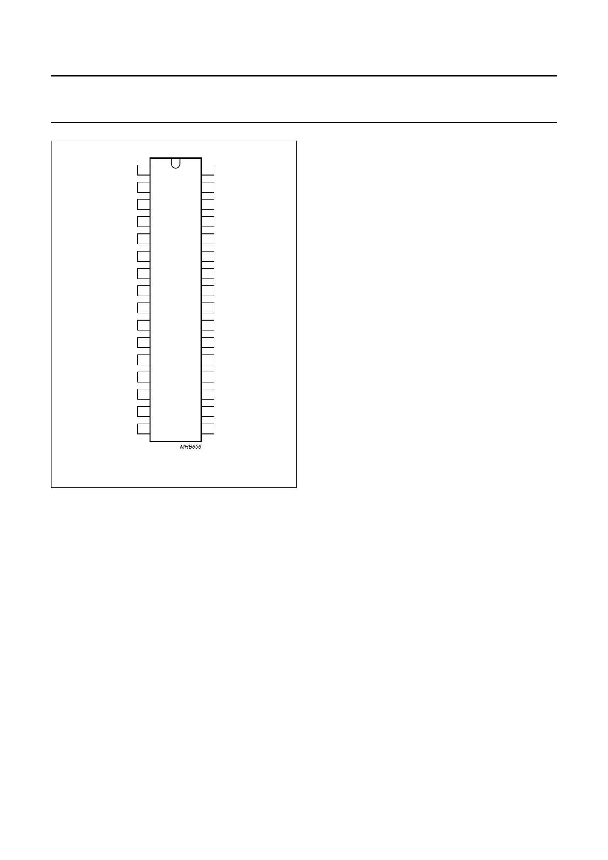
handbook, halfpage
HFLB 1
32 FOCUS
XRAY 2
31 HSMOD
BOP 3
30 HPLL2
BSENS 4
29 HCAP
BIN 5
28 HREF
BDRV 6
27 HBUF
PGND 7
26 HPLL1
HDRV 8
25 SGND
TDA4857PS
XSEL 9
24 VCAP
VCC 10
EWDRV 11
23 VREF
22 VAGC
VOUT2 12
21 VSMOD
VOUT1 13
20 ASCOR
VSYNC 14
19 SDA
HSYNC 15
18 SCL
CLBL 16
17 HUNLOCK
MHB656
Fig.2 Pin configuration.
FUNCTIONAL DESCRIPTION
Horizontal sync separator and polarity correction
HSYNC (pin 15) is the input for horizontal synchronization
signals, which can be DC-coupled TTL signals (horizontal
or composite sync) and AC-coupled negative-going video
sync signals. Video syncs are clamped to 1.28 V and
sliced at 1.4 V. This results in a fixed absolute slicing level
of 120 mV related to top sync.
For DC-coupled TTL signals the input clamping current is
limited. The slicing level for TTL signals is 1.4 V.
The separated sync signal (either video or TTL) is
integrated on an internal capacitor to detect and normalize
the sync polarity.
Normalized horizontal sync pulses are used as input
signals for the vertical sync integrator, the PLL1 phase
detector and the frequency-locked loop.
Vertical sync integrator
Normalized composite sync signals from HSYNC are
integrated on an internal capacitor in order to extract
vertical sync pulses. The integration time is dependent on
the horizontal oscillator reference current at HREF
(pin 28). The integrator output directly triggers the vertical
oscillator.
Vertical sync slicer and polarity correction
Vertical sync signals (TTL) applied to VSYNC (pin 14) are
sliced at 1.4 V. The output signal of the sync slicer is
integrated on an internal capacitor to detect and normalize
the sync polarity. The output signals of vertical sync
integrator and sync normalizer are disjuncted before they
are fed to the vertical oscillator.
Video clamping/vertical blanking generator
The video clamping/vertical blanking signal at CLBL
(pin 16) is a two-level sandcastle pulse which is especially
suitable for video ICs such as the TDA488x family, but also
for direct applications in video output stages.
The upper level is the video clamping pulse, which is
triggered by the horizontal sync pulse. Either the leading or
trailing edge can be selected by setting control bit CLAMP
via the I2C-bus. The width of the video clamping pulse is
determined by an internal single-shot multivibrator.
The lower level of the sandcastle pulse is the vertical
blanking pulse, which is derived directly from the internal
oscillator waveform. It is started by the vertical sync and
stopped with the start of the vertical scan. This results in
optimum vertical blanking. Two different vertical blanking
times are accessible, by control bit VBLK, via the I2C-bus.
Blanking will be activated continuously if one of the
following conditions is true:
Soft start of horizontal and B+ drive [voltage at HPLL2
(pin 30) pulled down externally or by the I2C-bus]
PLL1 is unlocked while frequency-locked loop is in
search mode or if horizontal sync pulses are absent
No horizontal flyback pulses at HFLB (pin 1)
X-ray protection is activated
Supply voltage at VCC (pin 10) is low (see Fig.23).
Horizontal unlock blanking can be switched off, by control
bit BLKDIS, via the I2C-bus while vertical blanking and
protection blanking is maintained.
2000 Jan 31
6
Share Link: 