UDA1345TS 데이터 시트보기 (PDF) - NXP Semiconductors.
부품명
상세내역
제조사
UDA1345TS Datasheet PDF : 29 Pages
| |||
NXP Semiconductors
Economy audio CODEC
Product specification
UDA1345TS
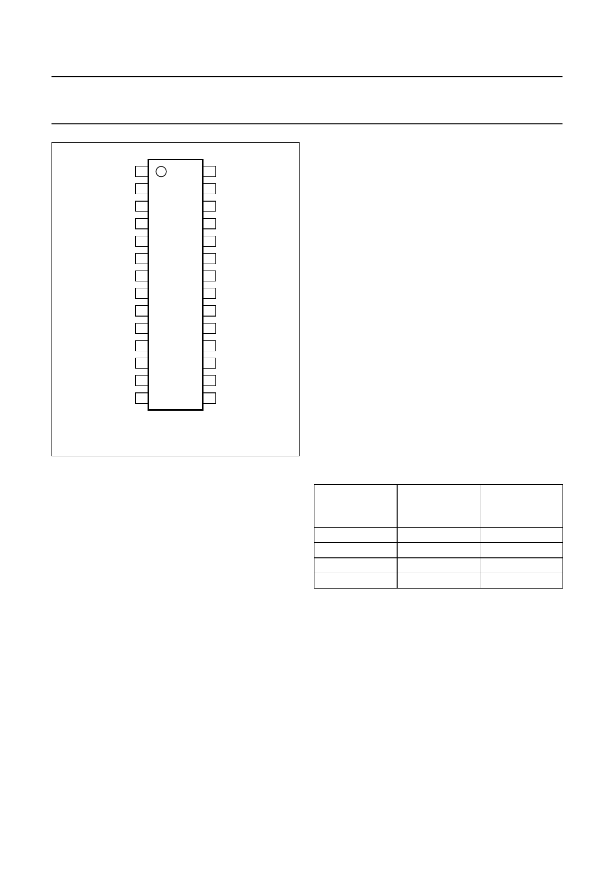
handbook, halfpage
VSSA(ADC) 1
VDDA(ADC) 2
VINL 3
28 Vref(D)
27 VSSO
26 VOUTL
Vref(A) 4
VINR 5
25 VDDO
24 VOUTR
VADCN 6
23 VDDA(DAC)
VADCP 7
22 VSSA(DAC)
UDA1345TS
MC1 8
21 MC2
MP1 9
20 MP5
VDDD 10
VSSD 11
SYSCLK 12
19 DATAI
18 DATAO
17 WS
MP2 13
16 BCK
MP3 14
15 MP4
MGS876
Fig.2 Pin configuration.
7.1 Analog-to-Digital Converter (ADC)
The stereo ADC of the UDA1345TS consists of two
5th-order Sigma-Delta modulators. They have a modified
Ritchie-coder architecture in a differential switched
capacitor implementation. The oversampling ratio is 64.
7.2 Analog front-end
The analog front-end is equipped with a selectable 0 dB or
6 dB gain block (the pin to select this mode is given in
Section 7.10). This block can be used in applications in
which both 1 V (RMS) and 2 V (RMS) input signals can be
input to the UDA1345TS.
In applications in which a 2 V (RMS) input signal is used,
a 12 kΩ resistor must be used in series with the input of the
ADC. This forms a voltage divider together with the internal
ADC resistor and ensures that only 1 V (RMS) maximum
is input to the IC. Using this application for a 2 V (RMS)
input signal, the switch must be set to 0 dB. When a
1 V (RMS) input signal is input to the ADC in the same
application, the gain switch must be set to 6 dB.
An overview of the maximum input voltages allowed
against the presence of an external resistor and the setting
of the gain switch is given in Table 1; the power supply
voltage is assumed to be 3 V.
7 FUNCTIONAL DESCRIPTION
The UDA1345TS accommodates slave mode only, this
means that in all applications the system devices must
provide the system clocks (being the system clock itself
and the digital audio interface signals).
The system clock must be locked in frequency to the audio
digital interface input signals.
The BCK clock can be up to 128fs, or in other words the
BCK frequency is 128 times the Word Select (WS)
frequency or less: fBCK ≤ 128 × fWS.
Important: the WS edge MUST fall on the negative edge
of the BCK at all times for proper operation of the digital I/O
data interface.
Note: the sampling frequency range is from 8 to 100 kHz,
however for the 512fs clock mode the sampling range is
from 8 to 55 kHz.
Table 1 Application modes using input gain stage
RESISTOR
(12 kΩ)
Present
Present
Absent
Absent
INPUT GAIN
SWITCH
0 dB
6 dB
0 dB
6 dB
MAXIMUM
INPUT
VOLTAGE
2 V (RMS)
1 V (RMS)
1 V (RMS)
0.5 V (RMS)
7.3 Decimation filter (ADC)
The decimation from 64fs to 1fs is performed in two stages.
The first stage realizes a 4th-order
s----i-n-----x-
x
characteristic.
This filter decreases the sample rate by 8. The second
stage consists of 2 half-band filters and a recursive filter,
each decimating by a factor of 2.
2002 May 28
8
Share Link: 