UPD178004GC-XXX-3B9 데이터 시트보기 (PDF) - NEC => Renesas Technology
부품명
상세내역
제조사
UPD178004GC-XXX-3B9 Datasheet PDF : 56 Pages
| |||
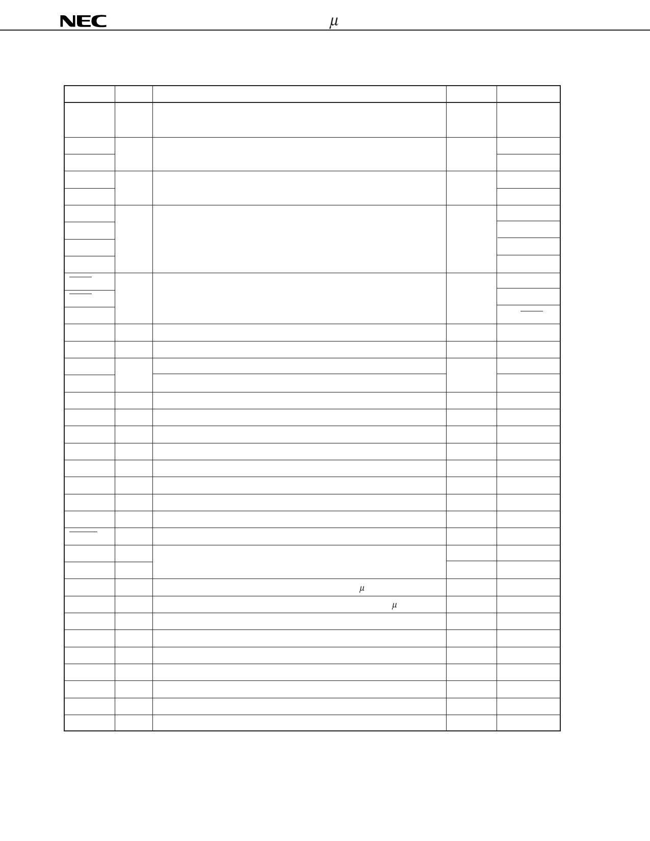
µPD178004, 178006, 178016, 178018
3.2 PINS OTHER THAN PORT PINS
Pin Name I/O
INTP0-INTP6 Input
SI0
Input
SI1
SO0
Output
SO1
SB0
I/O
SB1
SDA0
SDA1
SCK0
I/O
SCK1
SCL
STB
Output
BUSY
Input
TI1
Input
TI2
BEEP
Output
ANI0-ANI5 Input
PWM0-PWM2 Output
EO0, EO1 Output
VCOL
Input
VCOH
Input
AMIFC
Input
FMIFC
Input
RESET
Input
X1
Input
X2
—
REGOSC
—
REGCPU
—
VDD
—
GND
—
VDDPORT
—
GNDPORT —
VDDPLL
—
GNDPLL
—
IC
—
Function
After Reset Alternate Function
External maskable interrupt inputs with specifiable valid edges (rising Input
P00-P06
edge, falling edge, both rising and falling edges).
Serial interface serial data input
Input
P25/SB0/SDA0
P20
Serial interface serial data output
Input
P26/SB1/SDA1
P21
Serial interface serial data input/output
Input
P25/SI0/SDA0
P26/SO0/SDA1
P25/SI0/SB0
P26/SO0/SB1
Serial interface serial clock input/output
Input
P27/SCL
P22
P27/SCK0
Serial interface automatic transmit/receive strobe output
Input
P23
Serial interface automatic transmit/receive busy input
Input
P24
External count clock input to 8-bit timer (TM1)
Input
P33
External count clock input to 8-bit timer (TM2)
P34
Buzzer output
Input
P36
A/D converter analog input
Input
P10-P15
PWM output
—
P132-P134
Error out output from charge pump of the PLL frequency synthesizer
—
—
Inputs PLL local band frequency (In HF, MF mode)
—
—
Inputs PLL local band frequency (In VHF mode)
—
—
Inputs AM intermediate frequency counter
—
—
Inputs FM intermediate frequency counter
—
—
System reset input
—
—
System clock oscillation resonator connection
—
—
—
—
Oscillation regulator. Connected to GND via a 0.1-µF capacitor.
—
—
CPU power supply regulator. Connected to GND via a 0.1-µF capacitor.
—
—
Positive power supply
—
—
Ground
—
—
Positive power supply for port block
—
—
Ground for port block
—
—
Positive power supply for PLL
—
—
Ground for PLL
—
—
Internally connected. Connected to GND or GNDPORT.
—
—
10
Share Link: 