MC34080BDR2 데이터 시트보기 (PDF) - ON Semiconductor
부품명
상세내역
제조사
MC34080BDR2 Datasheet PDF : 16 Pages
| |||
MC34080 thru MC34085
APPLICATIONS INFORMATION
The bandwidth and slew rate of the MC34080 series is
nearly double that of currently available general purpose
JFET op–amps. This improvement in AC performance is due
to the P–channel JFET differential input stage driving a
compensated miller integration amplifier in conjunction with
an all NPN output stage.
The all NPN output stage offers unique advantages over
the more conventional NPN/PNP transistor Class AB output
stage. With a 10 k load resistance, the op amp can typically
swing within 1.0 V of the positive rail (VCC), and within 0.3 V
of the negative rail (VEE), providing a 28.7 p–p swing from
±15 V supplies. This large output swing becomes most
noticeable at lower supply voltages. If the load resistance is
referenced to VCC instead of ground, the maximum possible
output swing can be achieved for a given supply voltage. For
light load currents, the load resistance will pull the output to
VCC during the positive swing and the NPN output transistor
will pull the output very near VEE during the negative swing.
The load resistance value should be much less than that of
the feedback resistance to maximize pull–up capability.
The all NPN transistor output stage is also inherently
fast, contributing to the operation amplifier’s high
gain–bandwidth product and fast settling time. The
associated high frequency output impedance is 50 Ω (typical)
at 8.0 MHz. This allows driving capacitive loads from 0 pF to
300 pF without oscillations over the military temperature
range, and over the full range of output swing. The 55°C
phase margin and 7.6 dB gain margin as well as the general
gain and phase characteristics are virtually independent of
the sink/source output swing conditions. The high frequency
characteristics of the MC34080 series is especially useful for
active filter applications.
The common mode input range is from 2.0 V below the
positive rail (VCC) to 4.0 V above the negative rail (VEE). The
amplifier remains active if the inputs are biased at the positive
rail. This may be useful for some applications in that single
supply operation is possible with a single negative supply.
However, a degradation of offset voltage and voltage gain
may result.
Phase reversal does not occur if either the inverting or
noninverting input (or both) exceeds the positive common
mode limit. If either input (or both) exceeds the negative
common mode limit, the output will be in the high state. The
input stage also allows a differential up to ±44 V, provided the
maximum input voltage range is not exceeded. The supply
voltage operating range is from ±5.0 V to ±22 V.
For optimum frequency performance and stability, careful
component placement and printed circuit board layout should
be exercised. For example, long unshielded input or output
leads may result in unwanted input–output coupling. In order
to reduce the input capacitance, resistors connected to the
input pins should be physically close to these pins. This not
only minimizes the input pole for optimum frequency
response, but also minimizes extraneous “pickup” at
this node.
Supply decoupling with adequate capacitance close to the
supply pin is also important, particularly over temperature,
since many types of decoupling capacitors exhibit large
impedance changes over temperature.
Primarily due to the JFET inputs of the op amp, the input
offset voltage may change due to temperature cycling and
board soldering. After 20 temperature cycles (– 55° to
165°C), the typical standard deviation for input offset voltage
is 559 µV in the plastic packages. With respect to board
soldering (260°C, 10 seconds), the typical standard deviation
for input offset voltage is 525 µV in the plastic package.
Socketed devices should be used over a minimal
temperature range for optimum input offset voltage
performance.
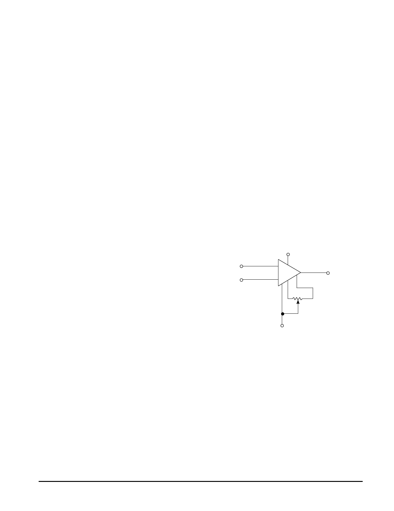
Figure 34. Offset Nulling Circuit
VCC
3+ 7
6
2–
5
1
4
5.0 k
VEE
MOTOROLA ANALOG IC DEVICE DATA
11
Share Link: 