N80C151SA 데이터 시트보기 (PDF) - Intel
부품명
상세내역
제조사
N80C151SA Datasheet PDF : 33 Pages
| |||
8XC151SA SB HIGH-PERFORMANCE CHMOS MICROCONTROLLER
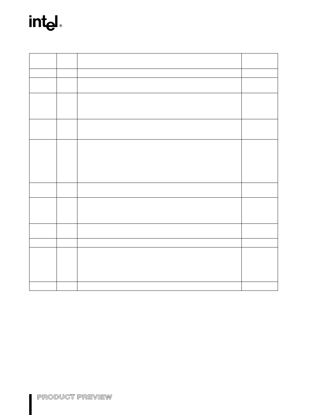
SIGNAL DESCRIPTIONS
Table 7 Signal Descriptions
Signal
Name
Type
Description
Multiplexed
With
A15 8
O Address Lines Upper address lines for the external bus
P2 7 0
AD7 0
I O Address Data Lines Multiplexed lower address lines and data lines
for external memory
P0 7 0
ALE
O Address Latch Enable ALE signals the start of an external bus
PROG
cycle and indicates that valid address information is available on lines
A15 8 and AD7 0 An external latch can use ALE to demultiplex the
address from the address data bus
CEX4 0
I O Programmable Counter Array (PCA) Input Output Pins These
are input signals for the PCA capture mode and output signals for the
PCA compare mode and PCA PWM mode
P1 6 3
P1 7
EA
I
External Access Directs program memory accesses to on-chip or
VPP
off-chip code memory For EA e 0 all program memory accesses
are off-chip For EA e 1 an access is to on-chip ROM OTPROM if
the address is within the range of the on-chip ROM OTPROM
otherwise the access is off-chip The value of EA is latched at
reset For devices without on-chip ROM OTPROM EA must be
strapped to ground
ECI
I
PCA External Clock Input External clock input to the 16-bit PCA
P1 2
timer
INT1 0
I
External Interrupts 0 and 1 These inputs set bits IE1 0 in the TCON
register If bits IT1 0 in the TCON register are set bits IE1 0 are set by
a falling edge on INT1 INT0 If bits INT1 0 are clear bits IE1 0
are set by a low level on INT1 0
P3 3 2
PROG
I
Programming Pulse The programming pulse is applied to this pin
ALE
for programming the on-chip OTPROM
P0 7 0
I O Port 0 This is an 8-bit open-drain bidirectional I O port
AD7 0
P1 0
P1 1
P1 2
P1 7 3
I O Port 1 This is an 8-bit bidirectional I O port with internal pullups
T2
T2EX
ECI
CEX3 0
CEX4
P2 7 0
I O Port 2 This is an 8-bit bidirectional I O port with internal pullups
A15 8
The descriptions of A15 8 P2 7 0 and AD7 0 P0 7 0 are for the nonpage-mode chip configuration (compatible with
44-lead PLCC and 40-pin DIP MCS 51 microcontrollers) If the chip is configured for page-mode operation port 0 carries
the lower address bits (A7 0) and port 2 carries the upper address bits (A15 8) and the data (D7 0)
9
Share Link: 