RDD05-03S1U 데이터 시트보기 (PDF) - CHINFA ELECTRONICS
부품명
상세내역
제조사
RDD05-03S1U Datasheet PDF : 4 Pages
| |||
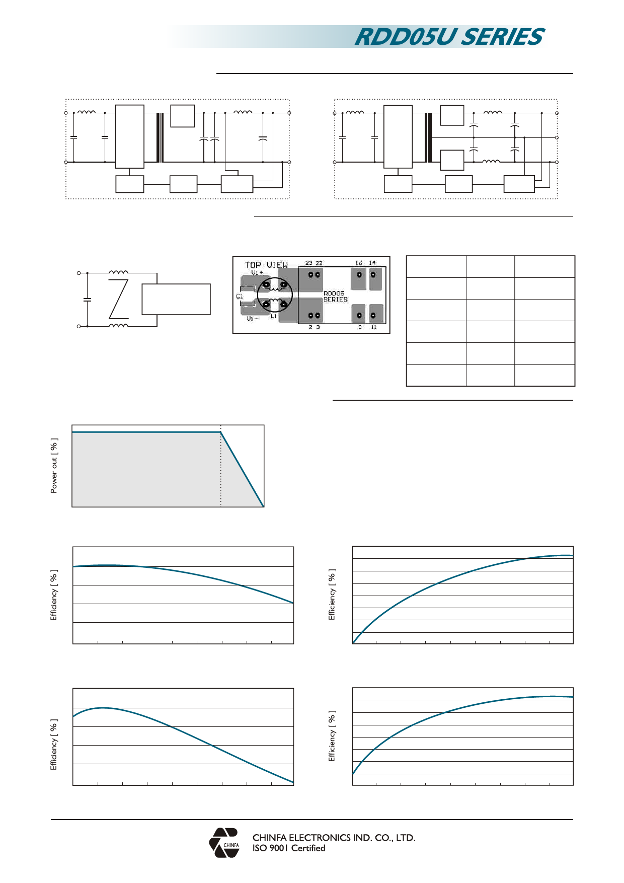
CIRCUIT SCHEMATIC
‧Block diagram for RDD05U series with single output
Vi +
Rectifier
Switching
Device
Vi -
PWM
Controller
Opto -
Isolation
Reference &
Error Amp.
RDD05U SERIES
SINGLE & DUAL OUTPUT
‧Block diagram for RDD05U series with dual output
Vo +
Vi +
Vo -
Vi -
Switching
Device
PWM
Controller
Rectifier
Rectifier
Opto -
Isolation
Reference &
Error Amp.
Vo +
com
Vo -
RECOMMENDED CIRCUIT
‧Recommended filter for EN55022 Class B compliance ‧Recommended EN 55022 Class B filter circuit layout.
‧The components used in the above figure, together with
the manufacturer part numbers for these components,
are as follows.
Vi +
C1
Vi -
L1
Vin +
Vo +
RDD05U
Vin -
Vo -
C1
L1
U
RDD05-XXX1U
2.2 μF / 50V
MLCC
1.5mH common
choke
RDD05-XXX2U
2.2 μF / 50V
MLCC
1.5mH common
choke
RDD05-XXX3U
2.2 μF / 100V
MLCC
1.5mH common
choke
RDD05-XXX4U
2.2 μF / 50V
MLCC
1.5mH common
choke
RDD05-XXX5U
2.2 μF / 100V
MLCC
1.5mH common
choke
DERATING AND EFFICIENCY CURVE
Temperature derating curve
100
Safe Operating Area
0
-40
71
100
Ambient Temperature [ oC ]
Efficiency Vs Input Voltage RDD05-05S2U
82
81
80
79
78
77
18 20 22
24 26 28 30
Input Voltage (V)
Io : Full Load
32 34 36
Efficiency Vs Input Voltage RDD05-05S4U
82
81
80
79
Io : Full Load
78
77
9 12 15 18 21 24 27 30 33 36
Input Voltage (V)
www.chinfa.com
2014.05.26
85
80
75
70
65
60
55
50
45
10
Efficiency Vs Output Load RDD05-05S2U
Vi : 24VDC
20 30 40 50 60 70 80 90 100
Output Load (%)
Efficiency Vs Output Load RDD05-05S4U
85
80
75
70
65
60
Vi : 24VDC
55
50
45
10 20 30
40 50 60 70 80 90 100
Output Load (%)
sales@chinfa.com
P4
Share Link: 