LV49157V 데이터 시트보기 (PDF) - ON Semiconductor
부품명
상세내역
제조사
LV49157V
ON Semiconductor

LV49157V Datasheet PDF : 30 Pages
| |||
LV49157V
Specifications
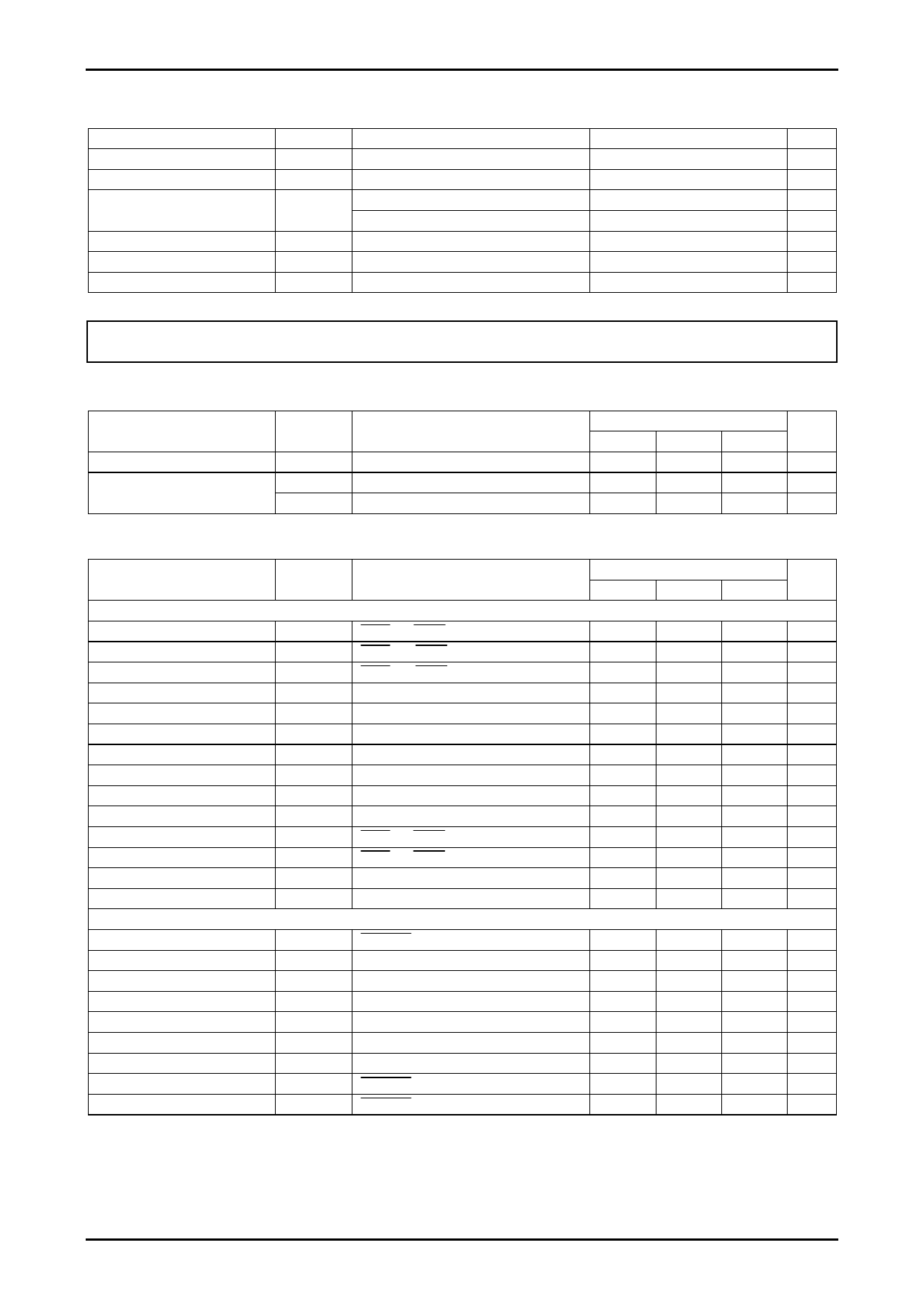
Absolute Maximum Ratings at Ta = 25°C
Parameter
Symbol
Conditions
Maximum supply voltage
VD
Supply voltage
Allowable power dissipation
Pd max
Our PCB, Soldered *
Package thermal resistance
θjc
Our PCB, Soldered *
Our PCB, Not soldered *
Maximum junction temperature
Tj max
Operating temperature
Topr
Storage temperature
Tstg
* : Mounted on a specified board 110.0mm × 100.0mm × 1.5mm, glass epoxy (two-layer)
Ratings
20
5
2.1
3.6
150
-25 to +75
-50 to +150
Unit
V
W
°C/W
°C/W
°C
°C
°C
Stresses exceeding Maximum Ratings may damage the device. Maximum Ratings are stress ratings only. Functional operation above the Recommended Operating
Conditions is not implied. Extended exposure to stresses above the Recommended Operating Conditions may affect device reliability.
Recommended Operating Range at Ta = 25°C
Parameter
Supply voltage range
Load impedance range
Symbol
VD
RL
RL(HP)
Conditions
Supply voltage
Speaker load
Headphone
min
9
4
Ratings
typ
15
8
16
Unit
max
18
V
Ω
Ω
Electrical Characteristics at Ta = 25°C, VD = 15V
Parameter
Symbol
Conditions
Main Amplifier (RL = 8Ω,L = 33μH (TOKO : A7502BY-330M), C = 0.1μF,CL=0.47μF)
Standby current
Ist
STBY = L, MUTE = L
Mute current
Imute
STBY = H, MUTE = L
Quiescent current
Voltage gain
Offset voltage
ICCO
VG
Voffset
STBY = H, MUTE = H
fin = 1kHz, VO = 0dBm
Rg = 0
Total harmonic distortion
Output power
Channel separation
Ripple rejection ratio
THD+N
PO
CH sep.
SVRR
PO = 1W, fin = 1kHz, AES17
THD+N = 10%, AES17
Rg = 0, VO = 0dBm, DIN AUDIO
fr = 100Hz, Vr = 0dBm, Rg = 0, DIN AUDIO
Noise
High-level input voltage
Low-level input voltage
Under voltage protection UPPER
VNO
VIH
VIL
UV_UPPER
Rg = 0, A-weight
STBY and MUTE pin
STBY and MUTE pin
VD voltage measure
Ratings
Unit
min
typ
max
1
14
20
35
45
28
30
-150
0.08
13
15
55
70
50
60
90
3
0
8.0
10 μA
26 mA
55 mA
32 dB
150 mV
0.4
%
W
dB
dB
300 μVrms
VD
V
1
V
V
Under voltage protection LOWER UV_LOWER VD voltage measure
7.0
V
Headphone Amplifier(RL = 16Ω,fin=1kHz)
Quiescent current
ICCO
Voltage gain
VG
Total harmonic distortion
THD+N
Output power
Channel separation
PO
CH sep.
Ripple rejection ratio
SVRR
HP_STBY = H
VO = -10dBm
PO = 10mW, DIN AUDIO
THD+N = 10%, DIN AUDIO
fin=1kHz, Rg = 0, VO = -10dBm, DIN AUDIO
fr = 100Hz, Vr = 0dBm, Rg = 0, DIN AUDIO
8
12 mA
9.5
11.5
13.5 dB
0.05
0.3
%
48
60
72
W
55
70
dB
55
70
dB
Noise
VNO
Rg = 0, A-weight
12
60 μVrms
High-level input voltage
VIH
HP_STBY pin
3
VD
V
Low-level input voltage
VIL
HP_STBY pin
0
1
V
Note : The values of these characteristics were measured in the Our test environment. The actual values in an end system will vary depending on the printed
circuit board pattern, the external components actually used, and other factors.
No.A1567-2/30
Share Link: