LV4924VH 데이터 시트보기 (PDF) - ON Semiconductor
부품명
상세내역
제조사
LV4924VH Datasheet PDF : 16 Pages
| |||
Continued from preceding page.
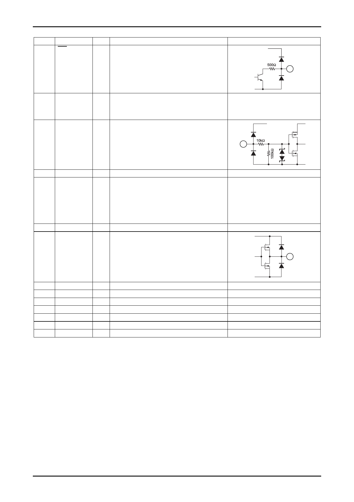
Pin No.
Pin name
I/O
3
SOS
I
LV4924VH
Description
Internal protection circuit detection output (OR output of the
thermal detection, over-current, voltage drop protection,
offset detection circuit) of an NPN open collector output type
4
NC1
5
NC2
6
NC3
7
NC4
8
PWM_A1
9
PWM_B1
10
PWM_B2
11
PWM_A2
-
Non connection
-
Non connection
-
Non connection
-
Non connection
I
PWM input (plus input) of OUT_CH1_P
I
PWM input (negative input) of OUT_CH1_N
I
PWM input (negative input) of OUT_CH2_N
I
PWM input (plus input) of OUT_CH2_P
FIN
12
13
14
15
16
17
18
19, 20
21, 22
26, 27
28, 29
33, 34
GND
NC5
NC6
NC7
NC8
NC9
NC10
NC11
PVD2
OUT_CH2_P
OUT_CH2_N
OUT_CH1_N
OUT_CH1_P
-
ground
-
Non connection
-
Non connection
-
Non connection
-
Non connection
-
Non connection
-
Non connection
-
Non connection
-
Power pin
O Output pin, Channel 2 plus
O Output pin, Channel 2 minus
O Output pin, Channel 1 minus
O Output pin, Channel 1 plus
23
24
25
30
31
32
35, 36
BOOT_CH2_P
VDDA2
BOOT_CH2_N
BOOT_CH1_N
VDDA1
BOOT_CH1_P
PVD1
I/O Bootstrap I / O pin, channel 2 plus
O Internal power supply decoupling capacitor connection
I/O Bootstrap I / O pin, channel 2 minus
I/O Bootstrap I / O pin, channel 1 minus
O Internal power supply decoupling capacitor connection
I/O Bootstrap I / O pin, channel 1 plus
-
Power pin
Equivalent Circuit
PVD
3
GND
PVD
GND
VDDA
PVD
GND
No.A1997-6/15
Share Link: 