PS21563-SP 데이터 시트보기 (PDF) - MITSUBISHI ELECTRIC
부품명
상세내역
제조사
PS21563-SP
MITSUBISHI ELECTRIC

PS21563-SP Datasheet PDF : 8 Pages
| |||
MITSUBISHI SEMICONDUCTOR <Dual-In-Line Package Intelligent Power Module>
PS21563-SP
TRANSFER-MOLD TYPE
INSULATED TYPE
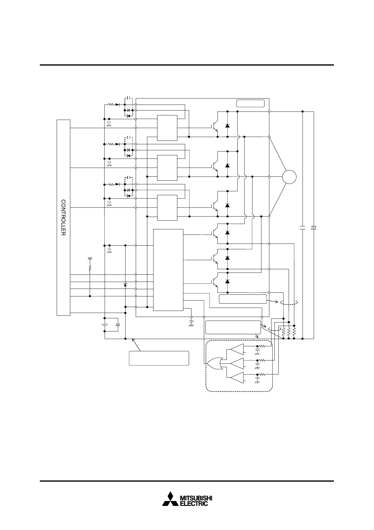
Fig. 6 TYPICAL DIP-IPM APPLICATION CIRCUIT EXAMPLE
C1:Tight tolerance temp-compensated electrolytic type C2,C3: 0.22~2µF R-category ceramic capacitor for noise filtering
C2 VUFB
C1 VUFS
VP1
C3
UP
C2 VVFB
C1 VVFS
VP1
C3
VP
C2 VWFB
C1 VWFS
VP1
C3
WP
HVIC1
VCC
VB
IN
HO
COM VS
HVIC2
VCC
VB
IN
HO
COM VS
HVIC3
VCC
VB
IN
HO
COM VS
DIP-IPM
P
U
V
M
W
LVIC
UOUT
VN1
NU
VCC
C3
5V line
VOUT
UN
VN
WN
Fo
VNC
UN
VN
WN
Fo
GND
WOUT
VNO
CIN
CFO
NV
C
NW
Too long wiring here might
cause short-circuit.
CFO CIN
VNO
15V line
C4(CFO)
A
Long GND wiring here might
generate noise to input and cause
IGBT malfunction.
If this wiring is too long, the SC
level fluctuation might be larger
and cause SC malfunction.
OR Logic
+
B R1
C5
- Vref
+
B R1
C5
- Vref
+
B R1
C5
- Vref
Shunt resistors
N1
Comparator
External protection circuit
Note 1 : To prevent the input signals oscillation, the wiring of each input should be as short as possible. (Less than 2cm)
2 : By virtue of integrating an application specific type HVIC inside the module, direct coupling to MCU terminals without any opto-coupler
or transformer isolation is possible.
3 : FO output is open drain type. This signal line should be pulled up to the positive side of the 5V power supply with approximately 10k Ω resistor.
4 : FO output pulse width is determined by the external capacitor between CFO and VNC terminals (CFO). (Example : CFO = 22 nF → tFO = 1.8 ms (typ.))
5 : The logic of input signal is high-active. The DIP-IPM input signal section integrates a 2.5kΩ (min) pull-down resistor. Therefore, when
using external filtering resistor, care must be taken to satisfy the turn-on threshold voltage requirement.
6 : To prevent malfunction of protection, the wiring of A, B, C should be as short as possible.
7 : Please set the C5R1 time constant in the range 1.5~2µs.
8 : Each capacitor should be located as nearby the pins of the DIP-IPM as possible.
9 : To prevent surge destruction, the wiring between the smoothing capacitor and the P, N1 pins should be as short as possible. Approxi-
mately a 0.1~0.22µF snubber capacitor between the P-N1 pins is recommended.
10 : To prevent ICs from surge destruction, it is recommended to insert a Zener diode (24V, 1W) between each control supply terminals.
11 : The reference voltage Vref of comparator should be set up the same rating of short circuit trip level (Vsc(ref): min.0.45V to max.0.52V).
12 : OR logic output level should be set up the same rating of short circuit trip level (Vsc(ref): min.0.45V to max.0.52V).
Jul. 2005
Share Link: