ICM7226B 데이터 시트보기 (PDF) - Intersil
부품명
상세내역
제조사
ICM7226B Datasheet PDF : 19 Pages
| |||
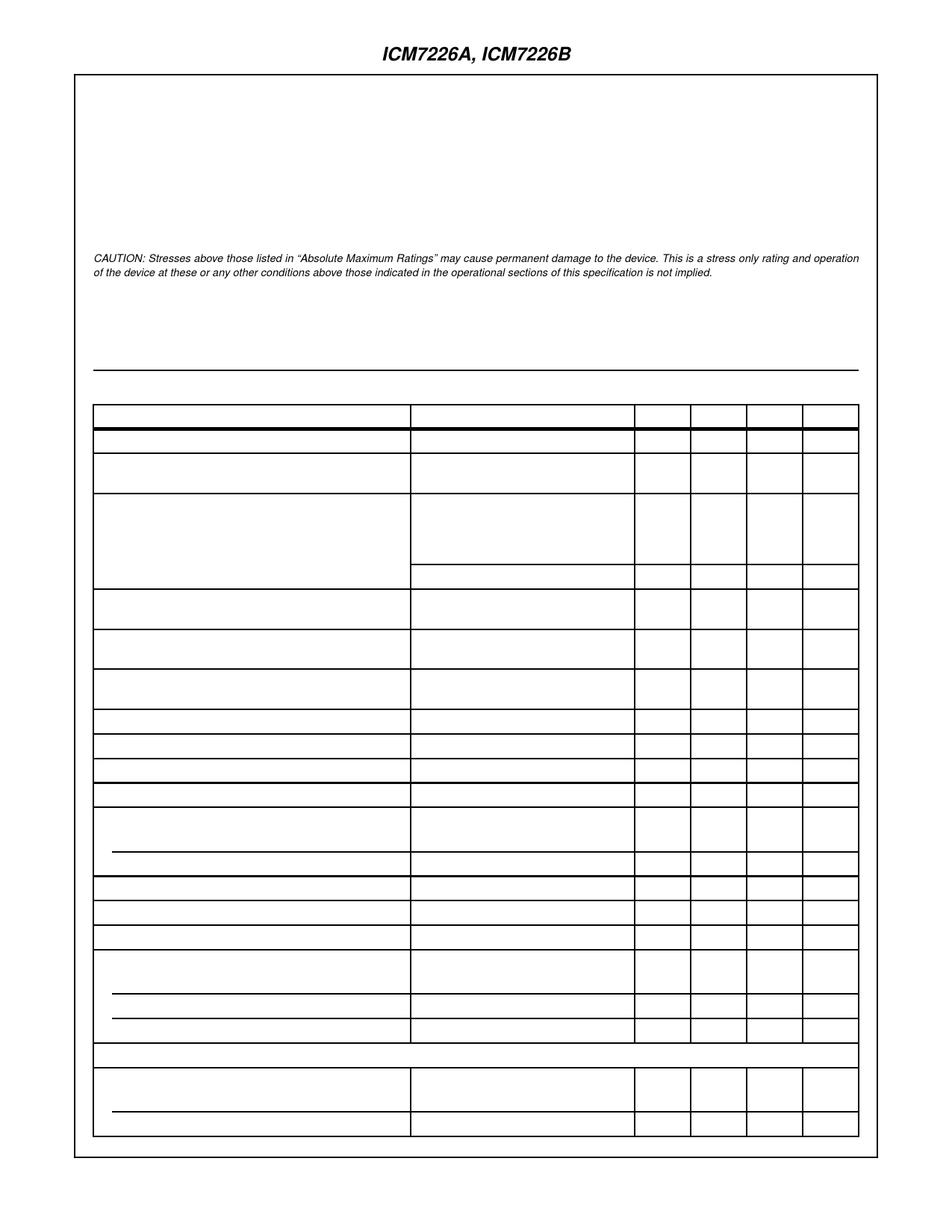
ICM7226A, ICM7226B
Absolute Maximum Ratings
Maximum Supply Voltage (VDD - VSS). . . . . . . . . . . . . . . . . . . . 6.5V
Maximum Digit Output Current . . . . . . . . . . . . . . . . . . . . . . . . 400mA
Maximum Segment Output Current . . . . . . . . . . . . . . . . . . . . . 60mA
Voltage On Any Input or
Output Terminal (Note 1) . . . . . . . . . . . . . . VDD +0.3V to VSS -0.3V
Operating Conditions
Temperature Range . . . . . . . . . . . . . . . . . . . . . . . . . . -25oC to 85oC
Thermal Information
Thermal Resistance (Typical, Note 2)
θJA (oC/W) θJC (oC/W)
CERDIP Package . . . . . . . . . . . . . . . .
45
9
PDIP Package . . . . . . . . . . . . . . . . . . .
50
N/A
Maximum Junction Temperature
CERDIP Package . . . . . . . . . . . . . . . . . . . . . . . . . . . . . . . . 175oC
PDIP Package . . . . . . . . . . . . . . . . . . . . . . . . . . . . . . . . . . . 150oC
Maximum Storage Temperature Range . . . . . . . . . .-55oC to 150oC
Maximum Lead Temperature (Soldering 10s) . . . . . . . . . . . . . 300oC
CAUTION: Stresses above those listed in “Absolute Maximum Ratings” may cause permanent damage to the device. This is a stress only rating and operation
of the device at these or any other conditions above those indicated in the operational sections of this specification is not implied.
NOTES:
1. Destructive latchup may occur if input signals are applied before the power supply is established or if inputs or outputs are forced to
voltages exceeding VDD or VSS by 0.3V.
2. θJA is measured with the component mounted on an evaluation PC board in free air.
Electrical Specifications VDD = 5.0V, TA = 25oC, Unless Otherwise Specified
PARAMETER
TEST CONDITIONS
Operating Supply Current, IDD
Supply Voltage Range (VDD -VSS), VSUPPLY
Maximum Frequency INPUT A, Pin 40, fA(MAX)
Display Off, Unused Inputs to VSS
-25oC to 85oC, INPUT A,
INPUT B Frequency at fMAX
-25oC to 85oC
4.75V < VDD < 6.0V, Figure 9
Function = Frequency, Ratio,
Unit Counter
Function = Period, Time Interval
Maximum Frequency INPUT B, Pin 2, fB(MAX)
Minimum Separation INPUT A to INPUT B,
Time Interval Function
Oscillator Frequency and External Oscillator Frequency,
fOSC
Oscillator Transconductance, gM
-25oC to 85oC
4.75V < VDD < 6.0V, Figure 10
-25oC to 85oC
4.75V < VDD < 6.0V, Figure 1
-25oC to 85oC
4.75V < VDD < 6.0V
VDD -4.75V, TA = 85oC
Multiplex Frequency, fMUX
fOSC = 10MHz
Time Between Measurements
fOSC = 10MHz
Input Rate of Charge, dVIN/dt
Inputs A, B
Input Voltages: Pins 2, 19, 33, 39, 40, 35
Input Low Voltage, VIL
-25oC to 85oC
Input High Voltage, VlH
Pins 2, 39, 40, Input Leakage, A, B, IILK
Input Resistance to VDD Pins 19, 33, RIN
VIN = VDD -1.0V
Input Resistance to VSS Pin 31, RIN
VIN = +1.0V
Output Current
Low Output Current, Pins 3, 5-7, 17, 18, 32, 38, IOL VOL = +0.4V
High Output Current, Pins 5-7, 17, 18, 32, HOL
VOH = +2.4V
High Output Current, Pins 3, 38, HOL
VOH = VDD -0.8V
ICM7226A
Segment Driver: Pins 8-11, 13-16
Low Output Current, IOL
High Output Current, IOH
VO = +1.5V
VO = VDD -1.0V
MIN
TYP MAX UNITS
-
2
5
mA
4.75
-
6.0
V
10
14
-
MHz
2.5
-
2.5
-
250
-
0.1
-
2000
-
-
500
-
200
-
15
-
-
3.5
-
-
-
100
400
50
100
400
-
100
-
265
-
-
MHz
-
MHz
-
ns
10
MHz
-
µS
-
Hz
-
ms
-
mV/µs
1.0
V
-
V
20
µA
-
kΩ
-
kΩ
-
µA
-
µA
-
µA
25
35
-
mA
-
100
-
µA
9-18
Share Link: 