GS71116AU-8I 데이터 시트보기 (PDF) - Unspecified
부품명
상세내역
제조사
GS71116AU-8I Datasheet PDF : 16 Pages
| |||
GS71116ATP/J/U
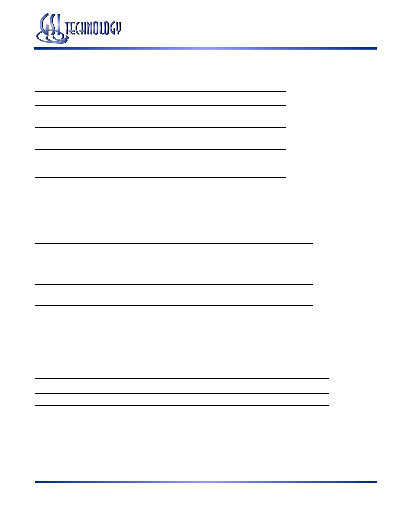
Absolute Maximum Ratings
Parameter
Symbol
Rating
Unit
Supply Voltage
VDD
Input Voltage
VIN
Output Voltage
VOUT
Allowable power dissipation
PD
Storage temperature
TSTG
–0.5 to +4.6
V
–0.5 to VDD +0.5
V
(≤ 4.6 V max.)
–0.5 to VDD +0.5
V
(≤ 4.6 V max.)
0.7
W
–55 to 150
oC
Note:
Permanent device damage may occur if Absolute Maximum Ratings are exceeded. Functional operation shall be restricted to Recommended
Operating Conditions. Exposure to higher than recommended voltages for extended periods of time could affect device reliability.
Recommended Operating Conditions
Parameter
Symbol Min
Typ
Max
Unit
Supply Voltage for -7/-8/-10/-12
VDD
3.0
3.3
3.6
V
Input High Voltage
VIH
2.0
—
VDD +0.3
V
Input Low Voltage
VIL
–0.3
—
0.8
V
Ambient Temperature,
Commercial Range
TAc
0
—
70
oC
Ambient Temperature,
Industrial Range
TAI
–40
—
85
oC
Notes:
1. Input overshoot voltage should be less than VDD +2 V and not exceed 20 ns.
2. Input undershoot voltage should be greater than –2 V and not exceed 20 ns.
Capacitance
Parameter
Input Capacitance
Output Capacitance
Symbol
Test Condition
Max
Unit
CIN
VIN = 0 V
5
pF
COUT
VOUT = 0 V
7
pF
Notes:
1. Tested at TA = 25°C, f = 1 MHz
2. These parameters are sampled and are not 100% tested.
Rev: 1.07 12/2004
4/16
Specifications cited are subject to change without notice. For latest documentation see http://www.gsitechnology.com.
© 2001, GSI Technology
Share Link: 