FDC40-48S05 데이터 시트보기 (PDF) - Power Mate Technology
부품명
상세내역
제조사
FDC40-48S05 Datasheet PDF : 3 Pages
| |||
Model
Number
FDC40-12S33
FDC40-12S05
FDC40-12S12
FDC40-12S15
FDC40-12D05
FDC40-12D12
FDC40-12D15
FDC40-12D3305
FDC40-12T0512
FDC40-12T0515
FDC40-24S33
FDC40-24S05
FDC40-24S12
FDC40-24S15
FDC40-24D05
FDC40-24D12
FDC40-24D15
FDC40-24D3305
FDC40-24T0512
FDC40-24T0515
FDC40-48S33
FDC40-48S05
FDC40-48S12
FDC40-48S15
FDC40-48D05
FDC40-48D12
FDC40-48D15
FDC40-48D3305
FDC40-48T0512
FDC40-48T0515
Input
Range
9 – 18 VDC
9 – 18 VDC
9 – 18 VDC
9 – 18 VDC
9 – 18 VDC
9 – 18 VDC
9 – 18 VDC
9 – 18 VDC
9 – 18 VDC
9 – 18 VDC
18 – 36 VDC
18 – 36 VDC
18 – 36 VDC
18 – 36 VDC
18 – 36 VDC
18 – 36 VDC
18 – 36 VDC
18 – 36 VDC
18 – 36 VDC
18 – 36 VDC
36 – 75 VDC
36 – 75 VDC
36 – 75 VDC
36 – 75 VDC
36 – 75 VDC
36 – 75 VDC
36 – 75 VDC
36 – 75 VDC
36 – 75 VDC
36 – 75 VDC
Output
Voltage
3.3 VDC
5 VDC
12 VDC
15 VDC
± 5 VDC
± 12 VDC
± 15 VDC
3.3 / 5VDC
5 / ± 12 VDC
5 / ± 15 VDC
3.3 VDC
5 VDC
12 VDC
15 VDC
± 5 VDC
± 12 VDC
± 15 VDC
3.3 / 5VDC
5 / ± 12 VDC
5 / ± 15 VDC
3.3 VDC
5 VDC
12 VDC
15 VDC
± 5 VDC
± 12 VDC
± 15 VDC
3.3 / 5VDC
5 / ± 12 VDC
5 / ± 15 VDC
Output
Current
10000mA
8000mA
3400mA
2700mA
+7000 / -1000mA
± 1800mA
± 1400mA
4000 / 4000mA
4000 / ± 850mA
4000 / ± 680mA
10000mA
8000mA
3400mA
2700mA
+7000 / -1000mA
± 1800mA
± 1400mA
4000 / 4000mA
4000 / ± 850mA
4000 / ± 680mA
10000mA
8000mA
3400mA
2700mA
+7000 / -1000mA
± 1800mA
± 1400mA
4000 / 4000mA
4000 / ± 850mA
4000 / ± 680mA
Note
1. The FDC40 series required a minimum 10% loading on the output to maintain
specified regulation. Operation under no-load condition will not damage these
devices, however they may not meet all listed specification.
2. Cross regulation:
Dual output—Asymmetrical load 25% to 100% full load
Triple output – 3.3V / 5V 100% load and one of auxiliary 100% load, other
auxiliary load change from 25% to 100% load
3. Simulated source impedance of 12uH. 12uH inductor in series with +Vin.
4. The ON-OFF control pin voltage is reference to negative input.
5. BELLCORE TR-NWT-000332. Case I: 50% Stress, Temperature at 40ºC.
(Ground fixed and controlled environment)
6. Maximum value at nominal input voltage and full load
7. Typical value at nominal input voltage and full load
8. Test by minimum Vin and constant resistor load.
Input
Current (6)
3530mA
4170mA
4100mA
4100mA
4330mA
4550mA
4430mA
3730mA
4490mA
4430mA
1720mA
2010mA
1980mA
2000mA
2130mA
2170mA
2140mA
1840mA
2180mA
2160mA
850mA
980mA
1000mA
1000mA
1060mA
1100mA
1100mA
910mA
1060mA
1060mA
Eff (7)
(%)
83
84
87
87
81
83
83
78
79
80
84
87
90
88
82
87
86
79
81
82
85
89
89
88
84
86
86
80
83
83
Capacitor (8)
Load max
25800uF
13600uF
2400uF
1550uF
12000 / 1700uF
± 1200uF
± 750uF
10300 / 6800uF
6800 / ± 590uF
6800 / ± 380uF
25800uF
13600uF
2400uF
1550uF
12000 / 1700uF
± 1200uF
± 750uF
10300 / 6800uF
6800 / ± 590uF
6800 / ± 380uF
25800uF
13600uF
2400uF
1550uF
12000 / 1700uF
± 1200uF
± 750uF
10300 / 6800uF
6800 / ± 590uF
6800 / ± 380uF
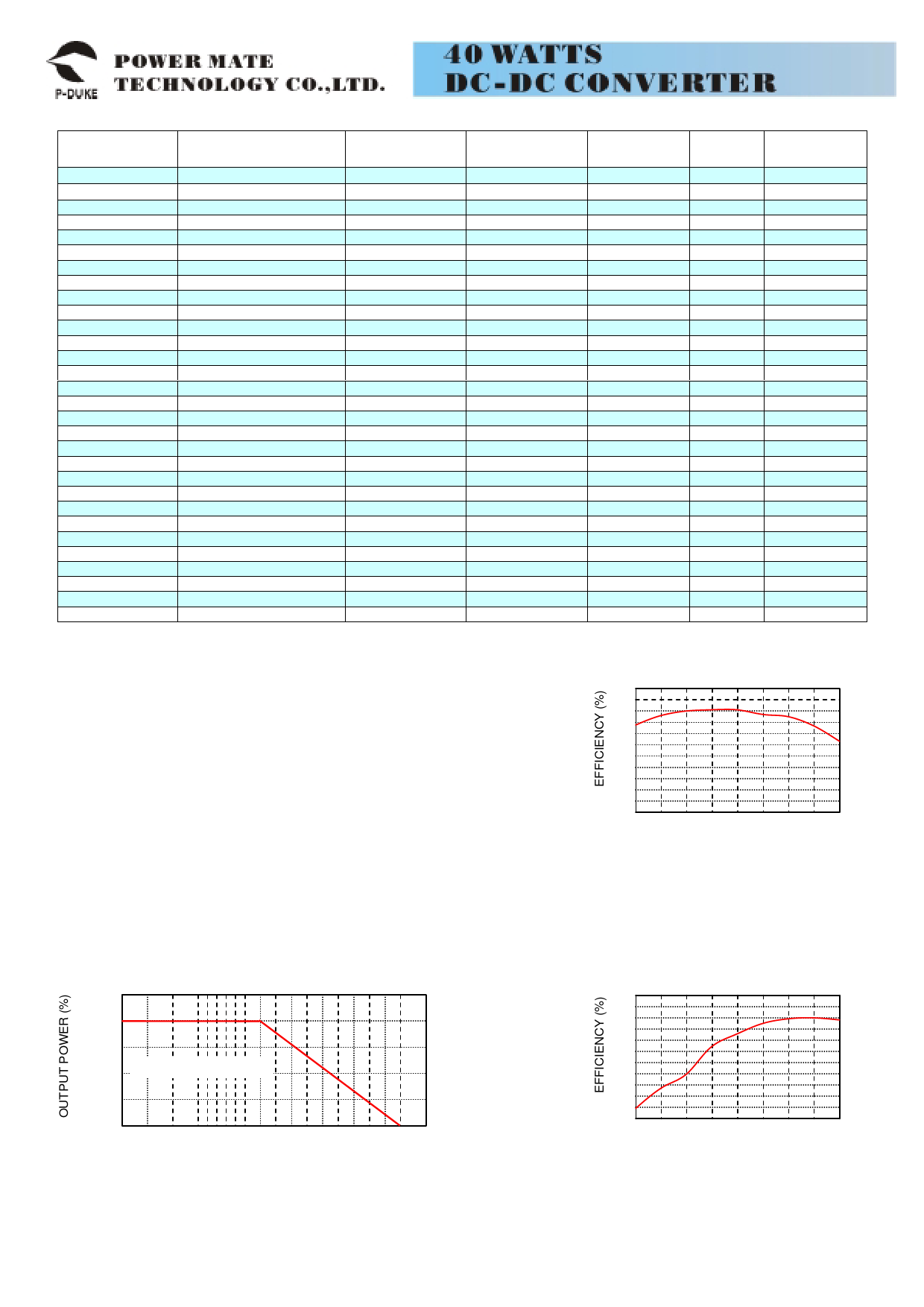
FDC40-48S05
Efficiency VS Input Voltage
90
89
88
87
86
85
84
83
82
81
80
36 40 45 50 55 60 65 70 75
INPUT VOLTAGE (V)
FDC40-48S05 Derating Curve
100
75
50 Nature convection
25
0
-40 -25 -10 0
50 60 70 80 90 100
AMBIENT TEMPERATURE (ºC)
FDC40-48S05
Efficiency VS Output load
90
89
88
86
84
82
80
70
60
50
45
0.5 1 2 3 4 5 6 7 8
OUTPUT LOAD (A)
Share Link: 