PI5V332Q 데이터 시트보기 (PDF) - Pericom Semiconductor Corporation
부품명
상세내역
제조사
PI5V332Q
Pericom Semiconductor Corporation

PI5V332Q Datasheet PDF : 7 Pages
| |||
PI5V332
Low On-Resistance Wideband/Video
Quad with Individual Control
Maximum Ratings
(Above which the useful life may be impaired. For user guidelines, not tested.)
Storage Temperature ............................................................. –65°C to +150°C
Ambient Temperature with Power Applied ............................ –40°C to +85°C
Supply Voltage to Ground Potential (Inputs & VCC Only)...... –0.5V to +7.0V
Supply Voltage to Ground Potential (Outputs & D/O Only) ... –0.5V to +7.0V
DC Input Voltage ..................................................................... –0.5V to +7.0V
DC Output Current................................................................................ 120mA
Note:
Stresses greater than those listed under MAXIMUM RAT-
INGS may cause permanent damage to the device. This is
a stress rating only and functional operation of the device
at these or any other conditions above those indicated in
the operational sections of this specification is not implied.
Exposure to absolute maximum rating conditions for ex-
tended periods may affect reliability.
Power Dissipation .................................................................................... 0.5W
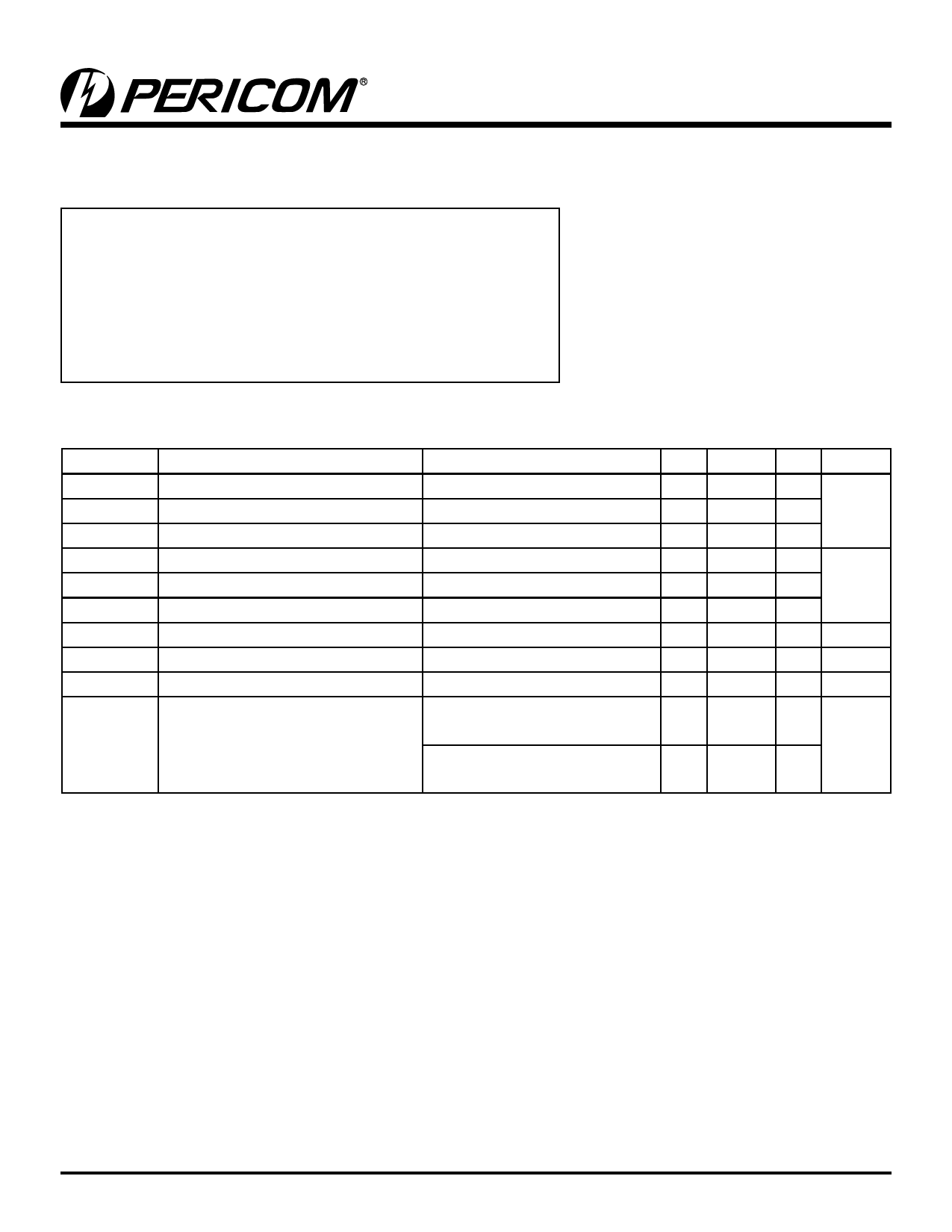
DC Electrical Characteristics (Over the Operating Range, TA = –40°C to +85°C, VCC = 5V ±5%)
Parameters
Description
Test Conditions(1)
Min. Typ(2) Max. Units
VANALOG
VIH
VIL
IIH
IIL
IO
VIK
IOS
VH
Analog Signal Range
Input HIGH Voltage
Input LOW Voltage
Input HIGH Current
Input LOW Current
Analog Output Leakage Current
Clamp Diode Voltage
Short Circuit Current(3)
Input Hysteresis at Control Pins
RON
Switch On-Resistance(4)
0
— 2.0
Guaranteed Logic HIGH Level
2.0
—
—
V
Guaranteed Logic LOW Level
–0.5 — 0.8
VCC = Max., VIN = VCC
—
—
±1
VCC = Max., VIN = GND
—
—
±1
µA
0 ≤ S1, S2 or D ≤ VCC, Switch Off —
—
±1
VCC = Min., IIN = –18 mA
— –0.7 –1.2 V
S1, S2, D = 0V VCC
100 —
—
mA
— 150 — mV
VCC = Min., VOUT = 0.975V
RL = 75Ω, ION = 13mA
VCC = MIN., VOUT = 1.95V
RL = 75Ω, ION = 26mA
—
3
7
Ω
—
7
10
Notes:
1. For Max. or Min. conditions, use appropriate value specified under Electrical Characteristics for the applicable device type.
2. Typical values are at VCC = 5.0V, TA = 25°C ambient and maximum loading.
3. Not more than one output should be shorted at one time. Duration of the test should not exceed one second.
4. Measured by the voltage drop between S1, S2, and D I/O pins at indicated current through the switch. On-Resistance is determined by the
lower of the voltages on the S1, S2, and D I/O pins. VOUT is the voltage across RL.
2
PS8118B
09/22/04
Share Link: