STK472-422A-E 데이터 시트보기 (PDF) - ON Semiconductor
부품명
상세내역
제조사
STK472-422A-E Datasheet PDF : 21 Pages
| |||
STK672-442A-E
Specifications
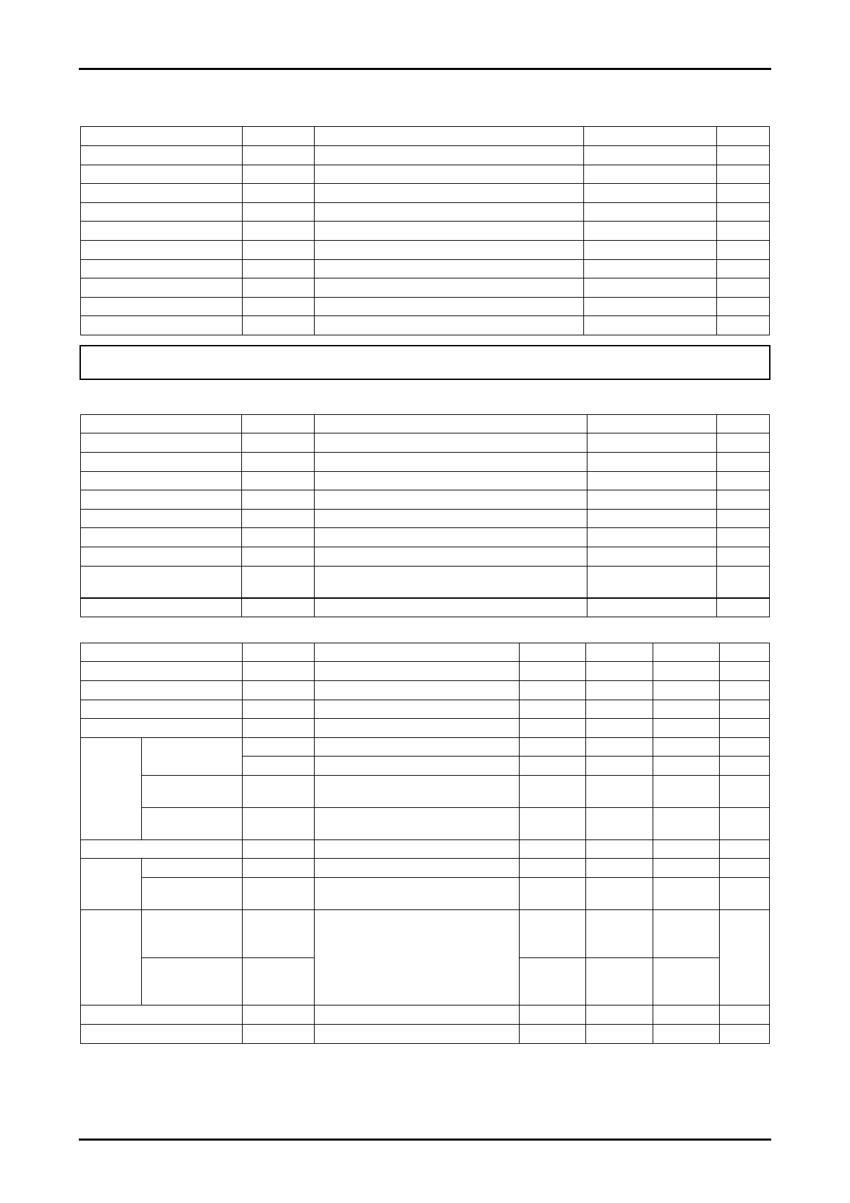
Absolute Maximum Ratings at Tc = 25°C
Parameter
Maximum supply voltage 1
Maximum supply voltage 2
Input voltage
Output current 1
Output current 2
Allowable power dissipation 1
Allowable power dissipation 2
Operating substrate temperature
Junction temperature
Storage temperature
Symbol
VCC max
VDD max
VIN max
IOP max
IOH max
PdMF max
PdPK max
Tc max
Tj max
Tstg
Conditions
No signal
No signal
Logic input pins
10μs, 1 pulse (resistance load)
VDD=5V, CLOCK≥200Hz
With an arbitrarily large heat sink. Per MOSFET
No heat sink
Ratings
unit
52
V
-0.3 to +6.0
V
-0.3 to +6.0
V
20
A
3.5
A
8.3
W
2.8
W
105
°C
150
°C
-40 to +125
°C
Stresses exceeding Maximum Ratings may damage the device. Maximum Ratings are stress ratings only. Functional operation above the Recommended Operating
Conditions is not implied. Extended exposure to stresses above the Recommended Operating Conditions may affect device reliability.
Allowable Operating Ranges at Ta=25°C
Parameter
Symbol
Conditions
Operating supply voltage 1
Operating supply voltage 2
VCC
VDD
With signals applied
With signals applied
Input high voltage
Input low voltage
Output current
CLOCK frequency
Phase driver withstand voltage
Recommended operating
substrate temperature
Recommended Vref range
VIH
VIL
IOH
fCL
VDSS
Tc
Vref
Pins 10, 11, 12, 13, 14, 15, 17
Pins 10, 11, 12, 13, 14, 15, 17
Tc=105°C, CLOCK≥200Hz
Minimum pulse width: at least 10μs
ID=1mA (Tc=25°C)
No condensation
Tc=105°C
Electrical Characteristics at Tc=25°C, VCC=24V, VDD=5.0V *1
Ratings
unit
10 to 42
V
5±5%
V
2.5 to VDD
V
0 to 0.8
V
3.0
A
0 to 50
kHz
100min
V
0 to 105
°C
0.2 to 1.8
V
Parameter
Symbol
Conditions
min
typ
max
unit
VDD supply current
Output average current *2
ICCO
Ioave
VDD=5.0V, ENABLE=Low
R/L=1Ω/0.62mH in each phase
5.7
7.0
mA
0.27
0.32
0.37
A
FET diode forward voltage
Vdf
If=1A (RL=23Ω)
1
1.6
V
Output saturation voltage
Vsat
RL=23Ω
0.25
0.38
V
Control
input pin
Input voltage
5V level input
current
VIH
Pins 10, 11, 12, 13, 14, 15, 17
VIL
Pins 10, 11, 12, 13, 14, 15, 17
Pins 10, 11, 12, 13, 14, 15, 17=5V
IILH
2.5
VDD
V
-0.3
0.8
V
50
75
μA
GND level input
current
Pins 10, 11, 12, 13, 14, 15, 17=GND
IILL
10
μA
Vref input bias current
FAULT1
pin
Output low voltage
5V level leakage
current
IIB
VOLF
IILF
Pin 19 =1.0V
Pin 16 (IO=5mA)
Pin 16 =5V
10
15
μA
0.25
0.5
V
10
μA
FAULT2 Overcurrent
Pin 8 (when all protection functions have
pin
detection output
VOF2
been activated)
voltage
Overheat
2.4
2.5
2.6
V
detection output
voltage
VOF3
3.1
3.3
3.5
Overheat detection temperature
TSD
Design guarantee
144
°C
PWM frequency
fc
41
48
55 kHz
Notes
*1: A fixed-voltage power supply must be used.
*2: The value for Ioave assumes that the lead frame of the product is soldered to the mounting circuit board.
Continued on next page.
No.A1587-2/21
Share Link: 