NJ88C33 데이터 시트보기 (PDF) - Zarlink Semiconductor Inc
부품명
상세내역
제조사
NJ88C33 Datasheet PDF : 14 Pages
| |||
NJ88C33
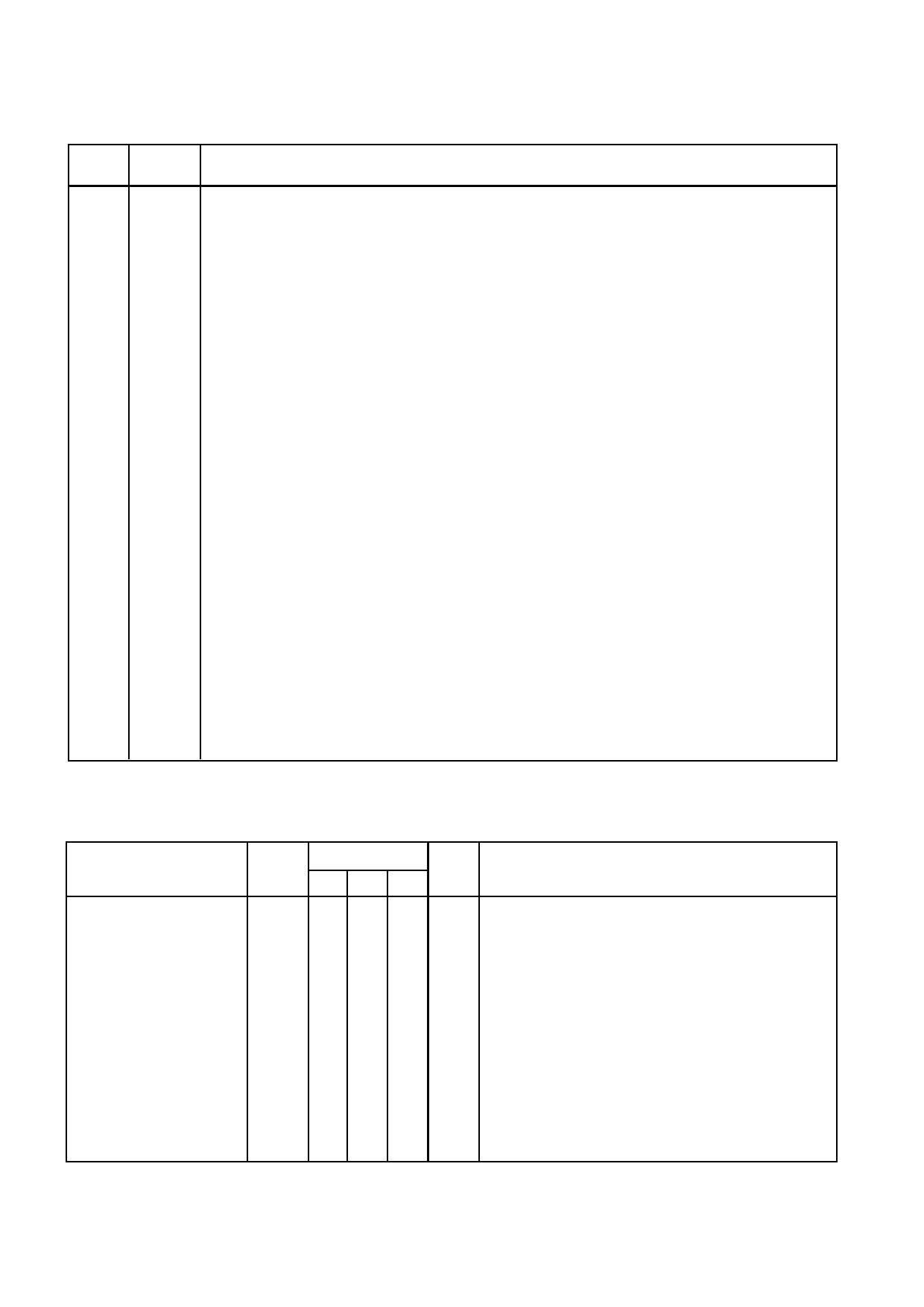
PIN DESIGNATIONS
Pin
Pin
No. Name
Description
1
VDD
Supply voltage (normally 5V or 3V).
2
RI
Reference frequency input from an accurate source, normally a crystal oscillator. The input is normally
an AC coupled sinewave but may be a DC coupled square wave.
3
S/D
Single/dual modulus operating mode selection input. Single modulus operation is selected by driving
the pin low. 'High' selects dual modulus mode.
4
SDA I2C bus data input pin. It is also an open-drain output for generating I2C bus acknowledge pulses.
5
SCL
I2C bus clock input. It can be clocked at up to 5MHz.
6
PORT Output control pin, which can be programmed via the I2C bus. It can be connected to the S/D pin to
select single or dual modulus mode under bus control.
7
MOD Modulus control pin. It is high in single modulus mode but switches in dual modulus operation. In dual
modulus mode, MOD remains low during operation of the A counter until A=0; MOD then remains high
until N=0, when both counters are reloaded. It can be programmed via the I2C bus as an open-drain
or push-pull output.
8
FI
Frequency input from a VCO or prescaler. The input is normally an AC coupled sinewave but may be
a DC coupled square wave.
9
GND2 Dedicated ground for the FI input buffer. It should be connected to the VCO ground or the prescaler
ground, if used. Any noise on this pin will affect the performance of the VCO loop.
10
FVN Open-drain output from the N counter.
11
GND1 Ground supply pin (global).
12
PD
Tristate current output from the phase detector. The polarity of the output can be programmed via the
I2C bus.
13
C
Voltage doubler output. The operation of the doubler can be controlled via the I2C bus. In applications
where the voltage doubler is switched off, this pin should be connected to GND1; a reservior capacitor
should be connected from this pin to GND1 for applications where it is switched on.
14
LD
Open-drain lock detect output - requires integration if used.
OPERATING RANGE
Test conditions (unless otherwise stated):
PLL locked, RI = 10MHz
Characteristic
Supply voltage
Ambient temperature
Supply current
Single modulus
Value
Symbol
Unit
Min. Typ. Max.
Conditions
VDD
2.5 5 5.5
V
Tamb
-40
+85 °C
IDD
2.1 3.0 mA FI = 50MHz, VFI = 150mVrms, N,R > 1000 without
voltage doubler, VDD = 5V, Tamb = 25°C
Dual modulus
IDD
2 3.0 mA FI = 10MHz, VFI = 500mVrms, N,R > 1000 without
voltage doubler, VDD = 5V, Tamb = 25°C
Standby mode
IDD
Standby mode
IDD
1
1.0 1.5
µA FI = 50MHz, VFI = 150mVrms, preamp off, divider off,
VDD = 5V, Tamb = 25°C
mA FI = 50MHz, VFI = 150mVrms, preamp on, divider off,
VDD = 5V, Tamb = 25°C
2
Share Link: 