NJ88C33 데이터 시트보기 (PDF) - Zarlink Semiconductor Inc
부품명
상세내역
제조사
NJ88C33 Datasheet PDF : 14 Pages
| |||
NJ88C33
VOLTAGE DOUBLER
Characteristic
Output Pin C
Output voltage
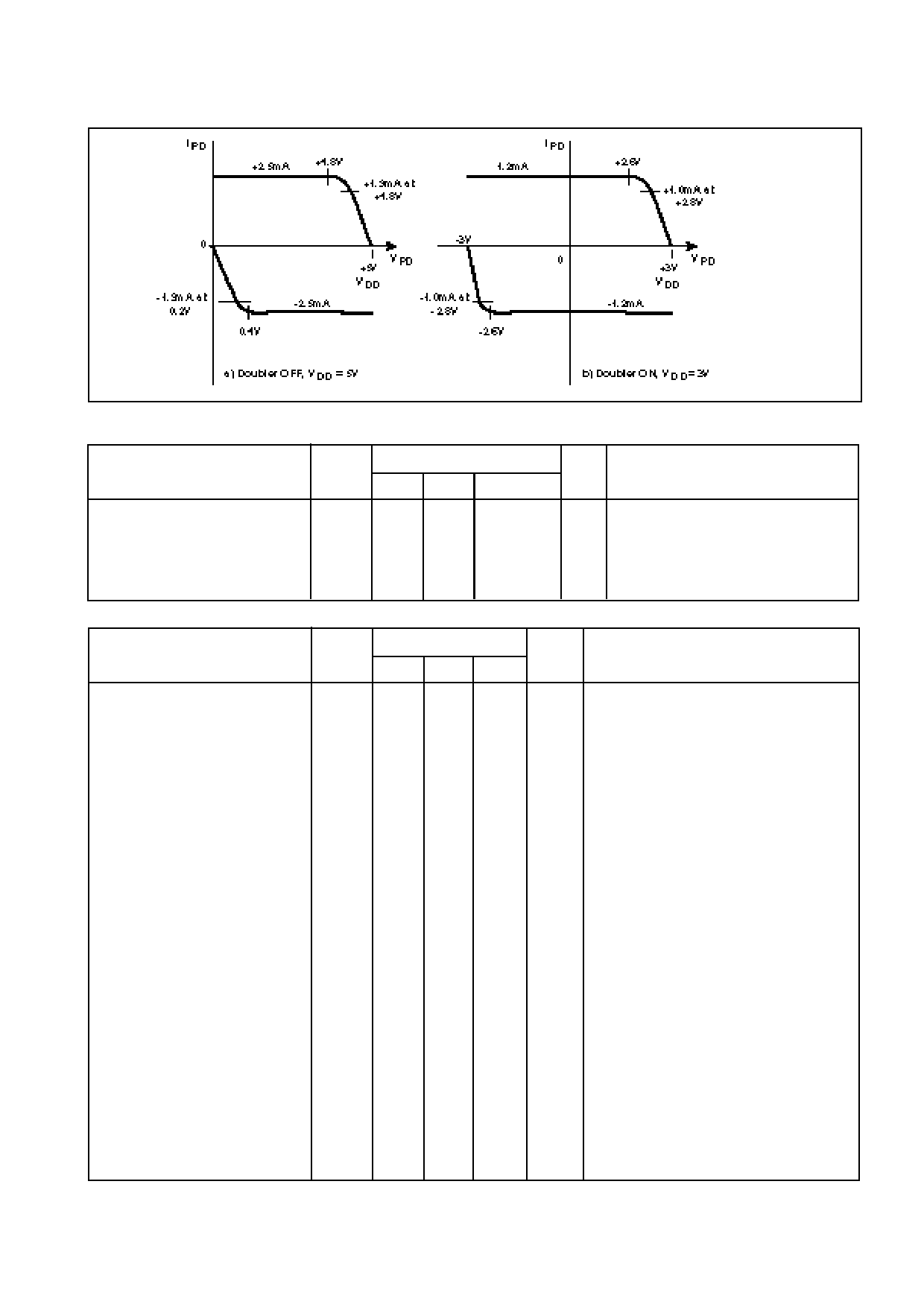
Fig. 4 Typical output signal PD, high current mode
VDD ≤ 3V
Value
Symbol
Unit
Min. Typ.
Max.
Conditions
VC
VC
-V
DD
-VDD
-VDD + 0.8V V
-VDD + 1.5V V
fVD = 2MHz, IOC = 0µA, VDD = 3V
fVD = 2MHz, IOC = 100µA, VDD = 3V
Current Consumption
TIMING INFORMATION
Characteristic
Input Signal RI
Input frequency
Input frequency
Rise time
Fall time
Slew rate
Input Signal FI
Input frequency
Input frequency
Rise time
Fall time
Slew rate
Input Signal FI
Input frequency
Input frequency
Rise time
Fall time
Slew rate
Output Signal PORT
Rise time
Fall time
Output Signal FVN
Fall time
Output Signal MOD
Rise time
Fall time
Delay time (L→H)
Delay time (H→L)
ID
100
µA fVD = 2MHz, IOC = 0µA, VDD = 3V
Value
Symbol
Unit
Min. Typ. Max.
Conditions
fmax
0
fmax
0
tR
tF
3
f
max
0
fmax
0
tR
tF
3
fmax
fmax
0
tR
0
tF
3
52 MHz
10
MHz VDD = 2.7V
1.5
µs
1.5
µs
V/µs
Dual modulus
52 MHz
20
MHz VDD = 2.7V
1.5
µs
1.5
µs
V/µs
Single modulus
150 MHz
52
MHz VDD = 2.7V
1.5
µs
1.5
µs
V/µs
tR
1
µs CL = 30pF
tF
1
µs CL = 30pF
tF
20
ns CL = 30pF
t
R
10
ns CL = 30pF
tF
10
ns CL = 30pF
tDLH
15
ns CL = 30pF Measured from +Ve edge of FI
tDHL
15
ns CL = 30pF Measured from +Ve edge of FI
5
Share Link: 