NAND04GW3C2N1E 데이터 시트보기 (PDF) - STMicroelectronics
부품명
상세내역
제조사
NAND04GW3C2N1E Datasheet PDF : 51 Pages
| |||
NAND04GA3C2A, NAND04GW3C2A
6 Device operations
The Ready/Busy signal can be used to monitor the start of the operation. During the latency
period the Ready/Busy signal goes Low, after this the Ready/Busy signal goes High, even if
the device is internally downloading page n+1.
Once the Cache Read operation has started, the Status Register can be read using the
Read Status Register command.
During the operation, SR5 can be read, to find out whether the internal reading is ongoing
(SR5 = ‘0’), or has completed (SR5 = ‘1’), while SR6 indicates whether the Cache Register
is ready to download new data.
To exit the Cache Read operation an Exit Cache Read command must be issued (see
Table 8).
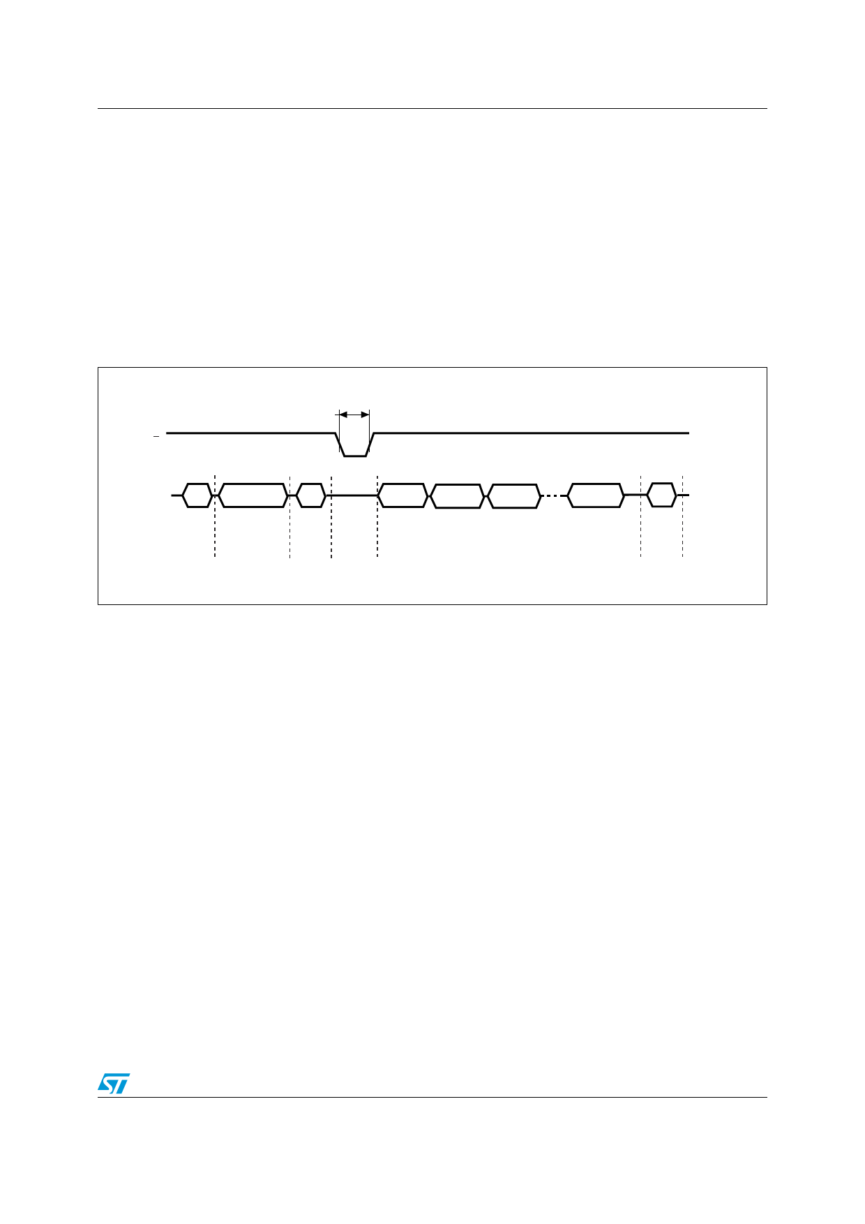
Figure 7. Cache Read Operation
tBLBH1
(Read Busy time)
RB
Busy
I/O
00h
Address
Inputs
31h
Read
Setup
Code
Cache
Read
Confirm
Code
1st page 2nd page 3rd page
Block N
last page
Data Output
34h
Exit
Cache
Read
Code
ai08661
6.5
Page Program
The Page Program operation is the standard operation to program data to the memory
array. Generally, data is programmed sequentially, however the device does support
Random Input within a page.
The memory array is programmed by page, however partial page programming is allowed
where any number of Bytes (1 to 2112) can be programmed.
Only one consecutive partial page program operations is allowed on the same page. After
exceeding this a Block Erase command must be issued before any further program
operations can take place in that page.
21/51
Share Link: 