NAND04GW3C2N1E 데이터 시트보기 (PDF) - STMicroelectronics
부품명
상세내역
제조사
NAND04GW3C2N1E Datasheet PDF : 51 Pages
| |||
NAND04GA3C2A, NAND04GW3C2A
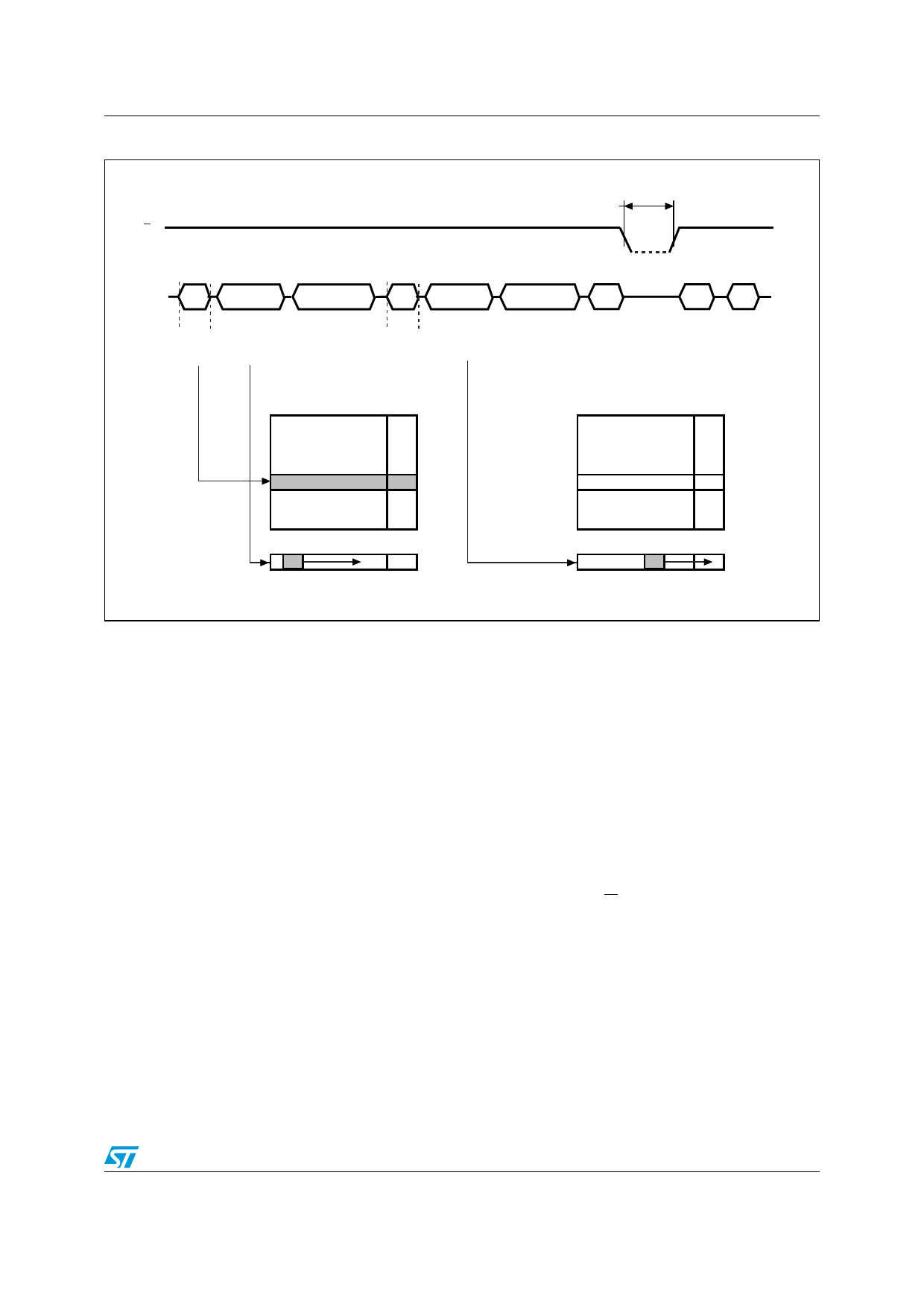
Figure 9. Random Data Input During Sequential Data Input
6 Device operations
RB
I/O
80h
Address
Inputs
Cmd
Code 5 Add cycles
Row Add 1,2,3 Col Add 1,2
Data Intput
85h
Cmd
Code
Address
Inputs
2 Add cycles
Col Add 1,2
tBLBH2
(Program Busy time)
Busy
Data Input 10h
Confirm
Code
70h SR0
Read Status Register
Main Area
Spare
Area
Main Area
Spare
Area
ai08664
6.8
Block Erase
Erase operations are done one block at a time. An erase operation sets all of the bits in the
addressed block to ‘1’. All previous data in the block is lost.
An erase operation consists of three steps (refer to Figure 10:
1. One bus cycle is required to setup the Block Erase command. Only addresses A19 to
A30 are used, the other address inputs are ignored.
2. Three bus cycles are then required to load the address of the block to be erased. Refer
to Table 7 for the block addresses of each device.
3. One bus cycle is required to issue the Block Erase confirm command to start the P/E/R
Controller.
The operation is initiated on the rising edge of write Enable, W, after the confirm command
is issued. The P/E/R Controller handles Block Erase and implements the verify process.
During the Block Erase operation, only the Read Status Register and Reset commands will
be accepted, all other commands will be ignored.
Once the program operation has completed the P/E/R Controller bit SR6 is set to ‘1’ and the
Ready/Busy signal goes High. If the operation completed successfully, the Write Status Bit
SR0 is ‘0’, otherwise it is set to ‘1’.
23/51
Share Link: 