SI3011-F-GS 데이터 시트보기 (PDF) - Silicon Laboratories
부품명
상세내역
제조사
SI3011-F-GS Datasheet PDF : 128 Pages
| |||
Si3050 + Si3011/18/19
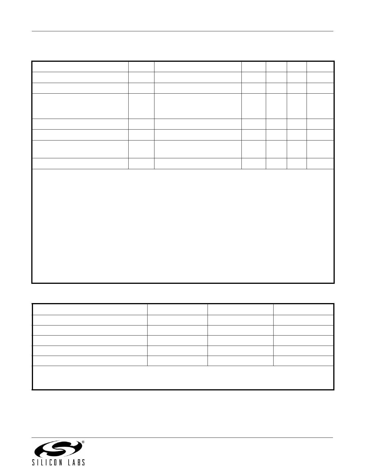
Table 4. AC Characteristics (Continued)
(VD = 3.0 to 3.6 V, TA = 0 to 70 °C, Fs = 8000 Hz, see "2. Typical Application Schematic" on page 17)
Parameter
Dynamic Range (Caller ID mode)8
Caller ID Full-Scale Level8
Symbol
DRCID
VCID
Gain Accuracy6,9
Transhybrid Balance10
Transhybrid Balance10
Two-Wire Return Loss
Test Condition
VIN = 1 kHz, –13 dBFS
2-W to DTX,
TXG2, RXG2, TXG3,
and RXG3 = 0000
300–3.4 kHz, ZACIM = ZLINE
1 kHz, ZACIM = ZLINE
300–3.4 kHz, all ac
terminations
Min
—
—
–0.5
Typ Max Unit
62 —
dB
1.5
— VPEAK
0 0.5
dB
20
——
dB
—
30 —
dB
25
——
dB
Two-Wire Return Loss
1 kHz, all ac terminations
—
32 —
dB
Notes:
1. Measured at TIP and RING with 600 termination at 1 kHz, as shown in Figure 1 on page 6.
2. With FULL = 1, the transmit and receive full-scale level of +3.2 dBm can be achieved with a 600 ac termination.
While the transmit and receive level in dBm varies with reference impedance, the DAA will transmit and receive 1 dBV
into all reference impedances. With FULL2 = 1, the transmit and receive full-scale level of +6.0 dBm can be achieved
with a 600 termination. In this mode, the DAA will transmit and receive +1.5 dBV into all reference impedances.
3. Receive full-scale level produces –0.9 dBFS at DTX.
4. DR = 20 x log (RMS VFS/RMS Vin) + 20 x log (RMS Vin/RMS noise). The RMS noise measurement excludes
harmonics. Here, VFS is the 0 dBm full-scale level per Note 1 above.
5. Measurement is 300 to 3400 Hz. Applies to both transmit and receive paths.
6. Vin = 1 kHz, –3 dBFS.
7. THD = 20 x log (RMS distortion/RMS signal).
8. DRCID = 20 x log (RMS VCID/RMS VIN) + 20 x log (RMS VIN/RMS noise). VCID is the 1.5 V full-scale level with the
enhanced caller ID circuit. With the typical CID circuit, the VCID full-scale level is 6 V peak, and the DRCID decreases to
50 dB.
9. Refer to Tables 10–11 for relative gain accuracy characteristics (passband ripple).
10. Analog hybrid only. ZACIM controlled by ACIM in Register 30.
Table 5. Absolute Maximum Ratings
Parameter
Symbol
Value
Unit
DC Supply Voltage
VD
–0.5 to 3.6
V
Input Current, Si3050 Digital Input Pins
IIN
±10
mA
Digital Input Voltage
VIND
–0.3 to (VD + 0.3)
V
Ambient Operating Temperature Range
TA
–40 to 100
°C
Storage Temperature Range
TSTG
–65 to 150
°C
Note: Permanent device damage can occur if the above Absolute Maximum Ratings are exceeded. Functional operation
should be restricted to the conditions as specified in the operational sections of this data sheet. Exposure to absolute
maximum rating conditions for extended periods might affect device reliability.
Rev. 1.5
9
Share Link: 