CD8227 데이터 시트보기 (PDF) - Unspecified
부품명
상세내역
제조사
CD8227 Datasheet PDF : 8 Pages
| |||
SUM
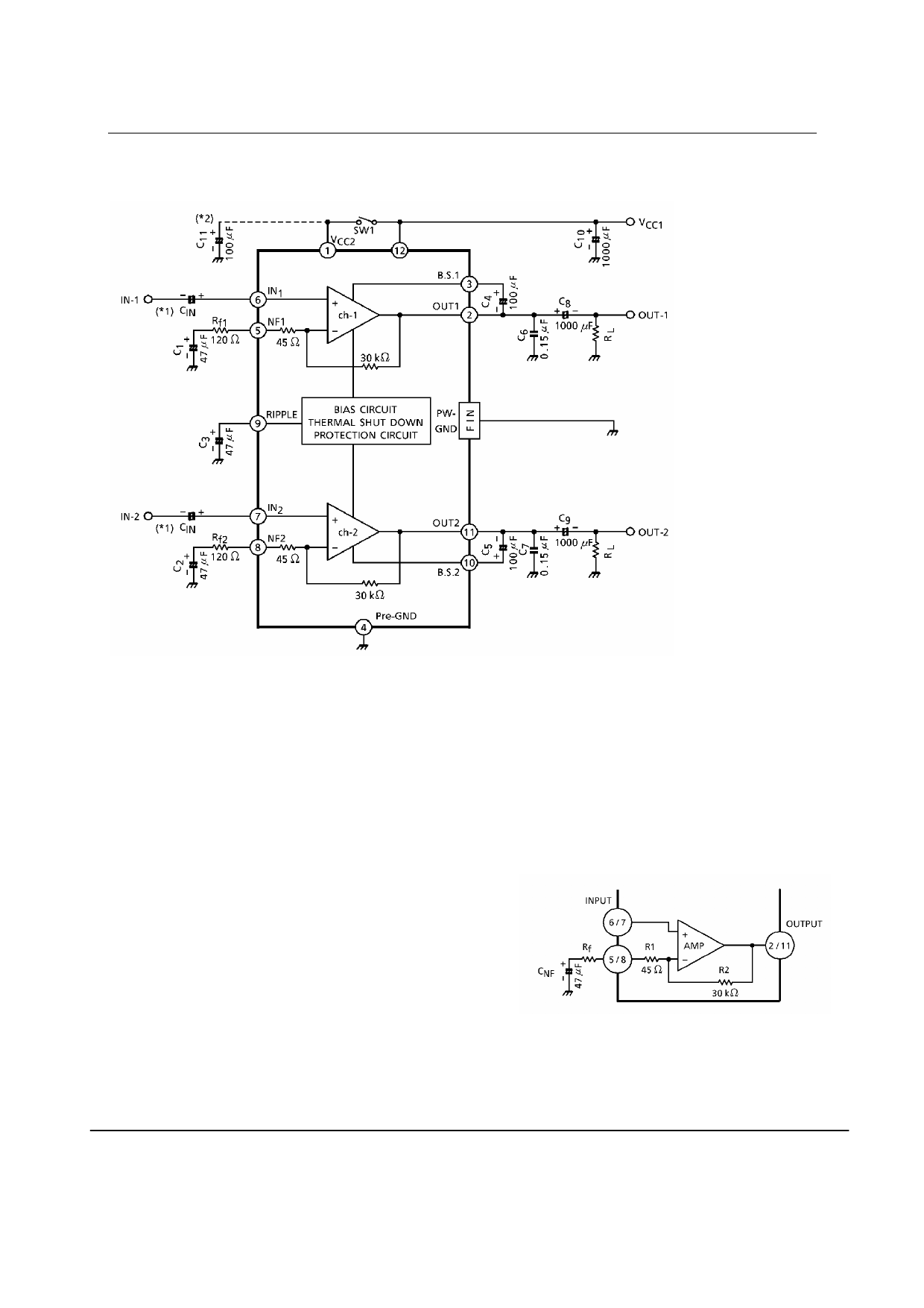
TEST CIRCUIT & BLOCK DIAGRAM
CD8227GP
*(1) This IC can be used without coupling capacitor (CIN),If volume slide noise occurred by
input offset voltage is undesirable, it needs to use the capacitor(CIN).
*(2) The condenser between the ④ pin and the GND(C11)is for reducing pop noise when the
power ON/OFF switch (SW1)is set to ON/OFF.
APPLICATION INFORMATION AND APPLICATION METHOD
1. ADJUSTMENT OF VOLTAGE GAIN
The voltage gain Gv is obtained as follows
by R1,R2 and Rf in Fig.1.
Gv=20log((Rf+R1+R2)/(Rf+R1))
When Rf=0 Gv=56.5dB(Typ.)
When Rf=120Ω Gv=45dB(Typ.)
By increasing Rf , reduction of Gv is possible ,
However, since the feedback
Fig 1.
increase is liable to produce oscillation , it is recommended to use this at 40dB or
over.
3/8
SUM
Share Link: 