1SMF5920BT1G(2010) 데이터 시트보기 (PDF) - ON Semiconductor
부품명
상세내역
제조사
1SMF5920BT1G Datasheet PDF : 4 Pages
| |||
1SMF5920BT1G
MAXIMUM RATINGS
Rating
Symbol
Value
Unit
DC Power Dissipation @ TA = 25°C (Note 1)
Derate above 25°C
Thermal Resistance, Junction−to−Ambient
°PD°
RqJA
350
°mW
2.9
mW/°C
350
°C/W
Thermal Resistance, Junction−to−Lead
RqJL
30
°C/W
Maximum DC Power Dissipation (Notes 1 and 2)
°PD
2.5
W
Operating and Storage Temperature Range
TJ, Tstg
−55 to +150
°C
Stresses exceeding Maximum Ratings may damage the device. Maximum Ratings are stress ratings only. Functional operation above the
Recommended Operating Conditions is not implied. Extended exposure to stresses above the Recommended Operating Conditions may affect
device reliability.
1. Mounted with recommended minimum pad size, PC board FR−4.
2. At lead temperature 75°C
ELECTRICAL CHARACTERISTICS (TA = 25°C unless
otherwise noted, VF = 1.5 V Max. @ IF = 200 mA for all
types)
Symbol
Parameter
IPP
VC
VRWM
IR
VBR
IT
IF
VF
Maximum Reverse Peak Pulse Current
Clamping Voltage @ IPP
Working Peak Reverse Voltage
Maximum Reverse Leakage Current @ VRWM
Breakdown Voltage @ IT
Test Current
Forward Current
Forward Voltage @ IF
I
IF
VC VBR VRWM
IIRT VF
V
IPP
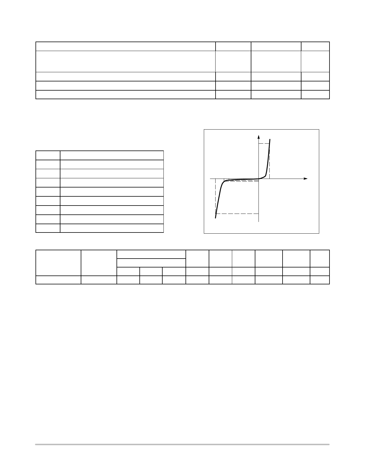
Uni−Directional TVS
ELECTRICAL CHARACTERISTICS (TL = 30°C unless otherwise noted, VF = 1.25 Volts @ 200 mA)
Device
Device
Marking
Zener Voltage (Note 3)
VZ @ IZT (Volts)
Min
Nom
Max
ZZT @ IZT ZZK @ IZK
IZT
IR @ VR
VR
(Note 4) (Note 4)
IZK
(mA)
(mA)
(V)
(W)
(W)
(mA)
1SMF5920BT1G
5Y2
5.89
6.2
6.51
60.5
5.0
4.0
2.0
200
1.0
3. Zener voltage is measured with the device junction in thermal equilibrium with an ambient temperature of 25°C.
4. Zener Impedance Derivation ZZT and ZZK are measured by dividing the AC voltage drop across the device by the AC current applied. The
specified limits are for IZ(ac) = 0.1 IZ(dc) with the ac frequency = 60 Hz.
http://onsemi.com
2
Share Link: 