NTE7081 데이터 시트보기 (PDF) - NTE Electronics
부품명
상세내역
제조사
NTE7081 Datasheet PDF : 3 Pages
| |||
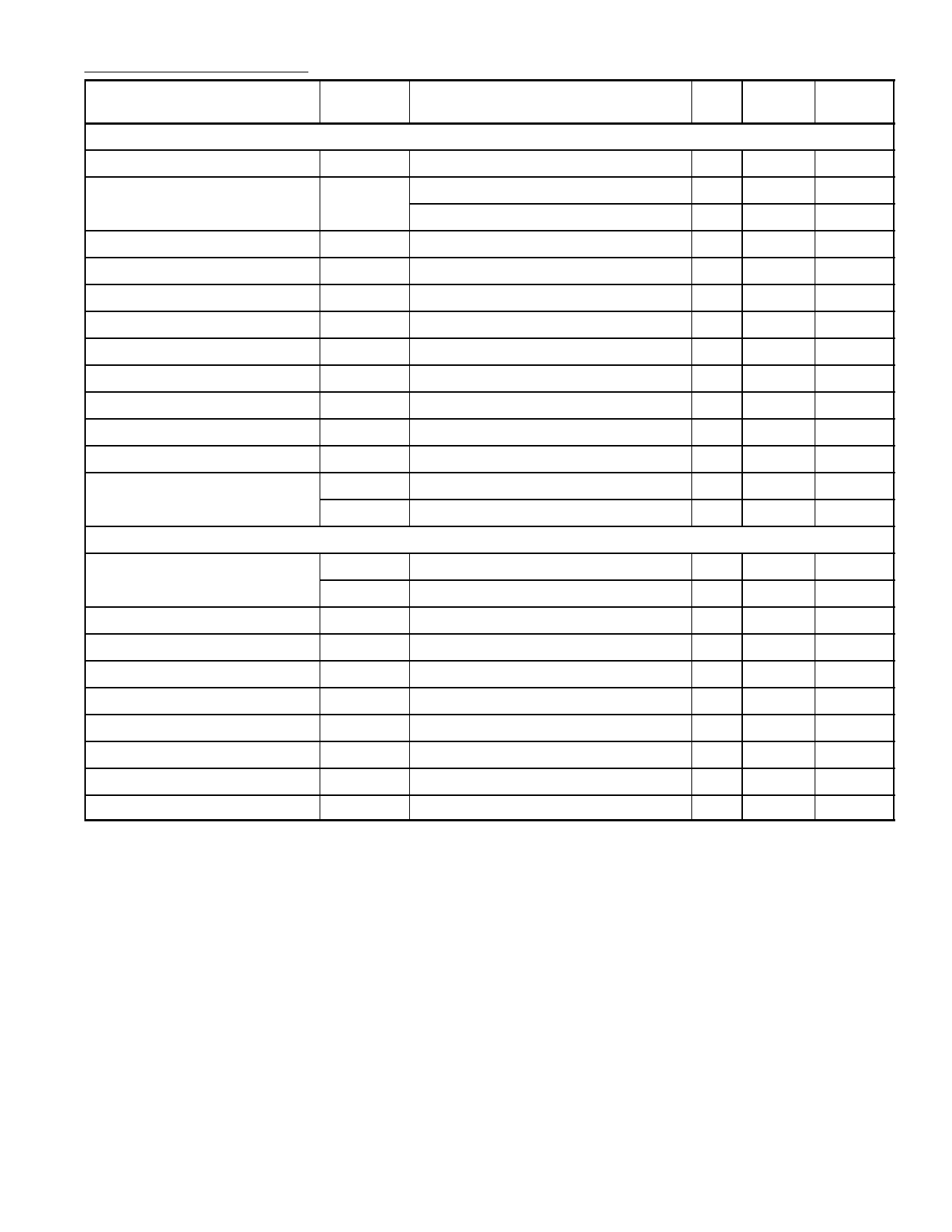
Electrical Characteristics: (TA = +25°C, VCC1 = VCC2 = 12V unless otherwise specified)
Parameter
Symbol
Test Conditions
Typ
Tested
(Note 3)
(Limits)
Unit
DC Static Test (S17, S21, S26 Open, V12 = 6V, V14 = 0V, V15 = 2V unless otherwise specified)
Supply Current
IS
VCC1 Only
73
90
Video Input Reference Voltage
V11
2.4 2.2
mA Max
VMIN
–
2.6
Video Input Bias Current
Ib
Any One Amplifier
5
20
Clamp Gate Low Input Voltage
V14L Clamp Comparators ON
1.2 0.8
Clamp Gate High Input Voltage
V14H Clamp Comparators OFF
1.6 2.0
Clamp Gate Low Input Current
I14L
V14 = 0V
–0.5 –5.0
Clamp Gate High Input Current
I14H
V14 = VCC
0.005 1.0
Clamp Cap Charge Current
Iclamp(+) V5, V8, or V10 = 0V
850
–
Clamp Cap Discharge Current
Iclamp(–) V5, V8, or V10 = 5V
–850 –
Video Output Low Voltage
VOL
V5, V8, or V10 = 0V
1.2
–
Video Output High Voltage
VOH
V5, V8, or V10 = 5V
8.9
–
Video Output Offset Voltage
∆VO(2V) Between Any Two Amplifiers, V15 = 2V ±0.5 ±50
∆VO(4V) Between Any Two Amplifiers, V15 = 4V ±0.5 ±50
AC Dymanic Test (S17, S21, S26 Closed, V14 = 0V, V15 = 4V, f = 10kHz unless otherwise specified)
Video Amplifier Gain
AVmax V12 = 12V, VIN = 560mVP–P
6.6
–
AVmid V12 = 5V, VIN = 560mVP–P
2.0
–
VMAX
µA Max
VMIN
VMAX
µA Max
µA Max
µA
µA
V
V
mV Max
mV Max
V/V
V/V
V12 for AV Low
Video Gain Match at AVmax
Video Gain Match at AVmid
Video Gain Match at AVlow
Video Amplifier Distortion
V12low
∆AVmax
∆AVmid
∆AVlow
THD
VIN = 1VP–P, Note 4
V12 = 12V, Note 5
V12 = 5V, Note 5
V12 = V12low, Note 4, Note 5
V12 = 3V, VIN = 1VP–P
2.0
–
V
±0.2
–
dB
±0.2
–
dB
±0.3
–
dB
0.5
–
%
Video Amplifier Bandwidth
f (–3dB) V12 = 12V, Note 6, Note 8
70
–
MHz
Video Amplifier, 10kHz Isolation Vsep10kHz V12 = 12V, Note 7
Video Amplifier, 10MHz Isolation Vsep10MHz V12 = 12V, Note 7, Note 8
–60
–
dB
–40
–
dB
Note 3. These parameters are guaranteed and 100% tested.
Note 4. Determine V12 low for –40dB attenuation of output. Reference AV to max.
Note 5. Measure gain difference between any two amplifiers. VIN = 1VP–P.
Note 6. Adjust input frequency, fIN, from 10kHz (AV max ref level) to the –3dB corner frequency
(f –3dB). VIN = 560mVP–P.
Note 7. VIN = 560mVP–P at fIN = 10kHz to any one amplifier. Measure output levels of the other two
undriven amplifiers relative to driven amplifier to determine channel separation. Terminate
the undriven amplifier inputs to simulate generator loading. Repeat test at fIN = 10MHz for
Vsep = 10MHz.
Note 8. Special test fixture without socket required.
Share Link: 