L6235PD 데이터 시트보기 (PDF) - STMicroelectronics
부품명
상세내역
제조사
L6235PD Datasheet PDF : 35 Pages
| |||
L6235
Pin connections
Package
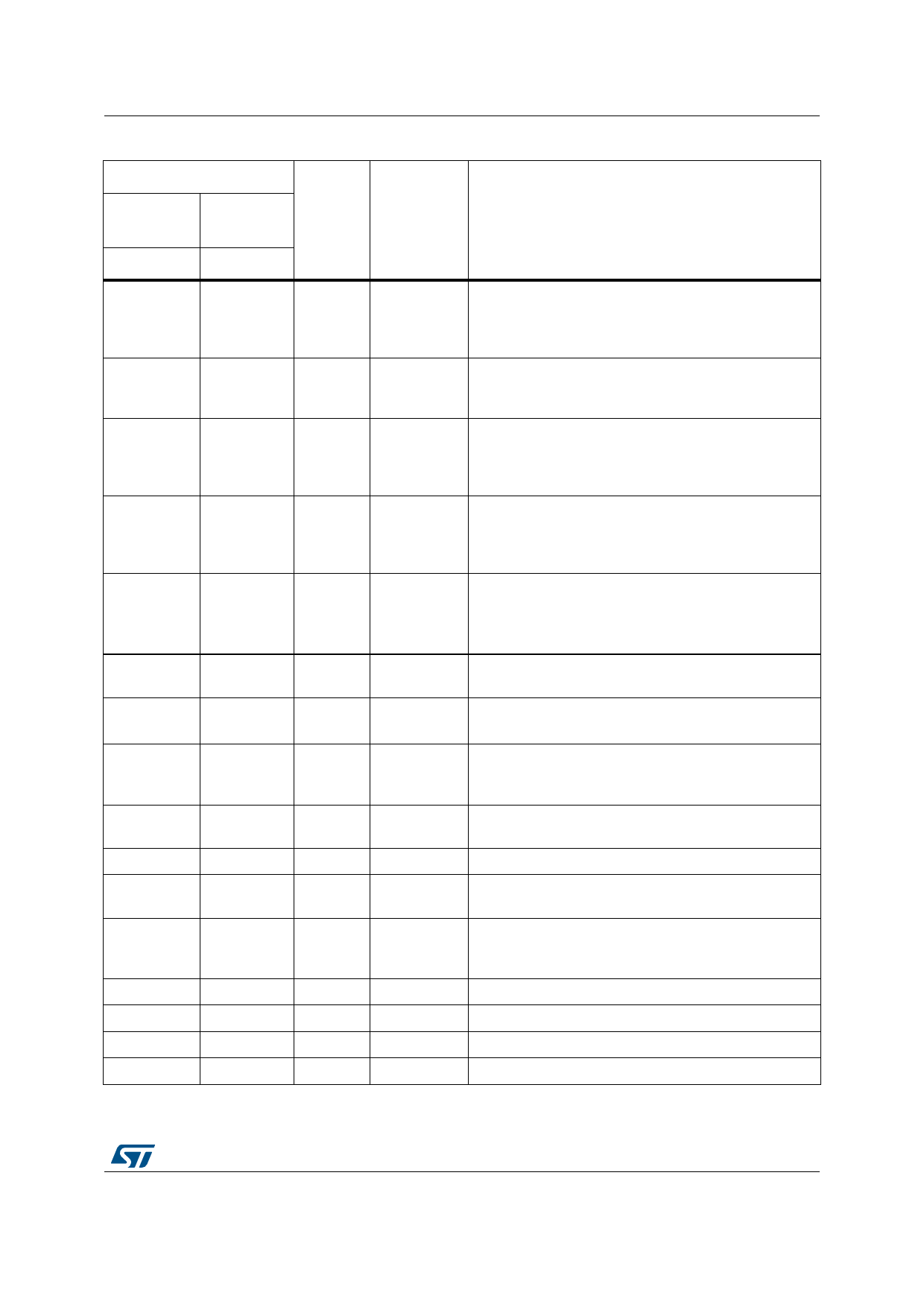
Table 4. Pin description (continued)
SO24/
PowerDIP24
PowerSO36
Name
Type
Function
Pin no.
Pin no.
6, 7, 18, 19
8
9
10
11
12
13
14
15
16
17
20
21
22
23
24
1, 18, 19, 36 GND
GND
Ground terminals. On PowerDIP24 and SO24
packages, these pins are also used for heat dissipation
toward the PCB. On PowerSO36 package the slug is
connected on these pins.
22
TACHO
Open drain
output
Frequency-to-voltage open drain output. Every pulse
from pin H1 is shaped as a fixed and adjustable length
pulse.
RC network pin. A parallel RC network connected
24
RCPULSE RC pin
between this pin and ground sets the duration of the
monostable pulse used for the frequency-to-voltage
converter.
Half-bridge 3 source pin. This pin must be connected
25
SENSEB
Power supply
together with pin SENSEA to power ground through
a sensing power resistor. At this pin also the inverting
input of the sense comparator is connected.
Selects the direction of the rotation. HIGH logic level
26
FWD/REV Logic input
sets forward operation, whereas LOW logic level sets
reverse operation.
If not used, it has to be connected to GND or +5 V.
27
EN
Logic input
Chip enable. LOW logic level switches OFF all Power
MOSFETs. If not used, it has to be connected to +5 V.
28
VREF
Logic input
Current controller reference voltage.
Do not leave this pin open or connect to GND.
Brake input pin. LOW logic level switches ON all high-
29
BRAKE Logic input
side Power MOSFETs, implementing the brake
function. If not used, it has to be connected to +5 V.
30
VBOOT
Supply
voltage
Bootstrap voltage needed for driving the upper Power
MOSFETs.
32
OUT3 Power output
Output 3.
33
VSB
Power supply
Half-bridge 3 power supply voltage. It must be
connected to the supply voltage together with pin VSA.
Half-bridge 1 and half-bridge 2 power supply voltage. It
4
VSA Power supply must be connected to the supply voltage together with
pin VSB.
5
OUT2 Power output
Output 2.
7
VCP
Output
Charge pump oscillator output.
8
H2
Sensor input
Single ended hall effect sensor input 2.
9
H3
Sensor input
Single ended hall effect sensor input 3.
DocID7618 Rev 2
7/35
35
Share Link: 