CXA2040 데이터 시트보기 (PDF) - Sony Semiconductor
부품명
상세내역
제조사
CXA2040 Datasheet PDF : 22 Pages
| |||
CXA2040Q
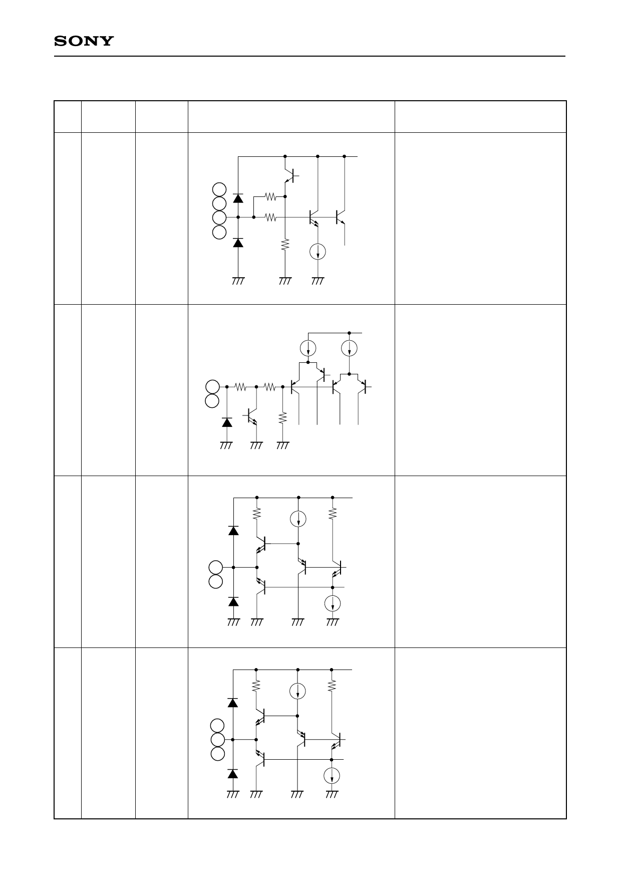
Pin Description
Pin
No.
Symbol Pin voltage
Equivalent circuit
Description
1 Y1
5 Y2
3 C1
7 C2
4.5V
1
20k
5
147
3
7
×2
28k
VCC
Y/C separation signal inputs.
Biased to approximately 4.5V.
Input the input signals through
capacitors. Connect protective
resistor of 220Ω between these
pins and the capacitors.
Y1 and Y2 pins: Luminance
signals input.
C1 and C2 pins: Chrominance
signals input.
4 S1
6 S2
50k 50k
4
6
100k
×4
VCC Applying a DC voltage to S1 and
S2 pins allows these voltages to
be applied to the microcomputer
as the I2C bus status register data.
S1, S2 = 0 to 2V
OPEN = 0, SEL = 1
S1, S2 = 4.75 to 7.25V
OPEN = 0, SEL = 0
S1, S2 = 9.5 to 12V
OPEN = 1, SEL = 0
11 YOUT
9 COUT
4.5V
200
×5
11
9
×6
VCC
1.2k
×2
×2
Y/C signal outputs.
YOUT pin: Luminance signal
output.
COUT pin: Chrominance signal
output.
17 CVOUT1
15 CVOUT2
13 CVOUT3
4.5V
200
17 × 5
15
13 × 6
VCC
1.2k
×2
×2
Composite video signal outputs.
CVOUT1, CVOUT2:
0dB output with respect to
the input signal.
CVOUT2:
+6dB output with respect
to the input signal.
–3–
Share Link: 