NCS37012MNTWG(2016) 데이터 시트보기 (PDF) - ON Semiconductor
부품명
상세내역
제조사
NCS37012MNTWG Datasheet PDF : 9 Pages
| |||
NCS37012
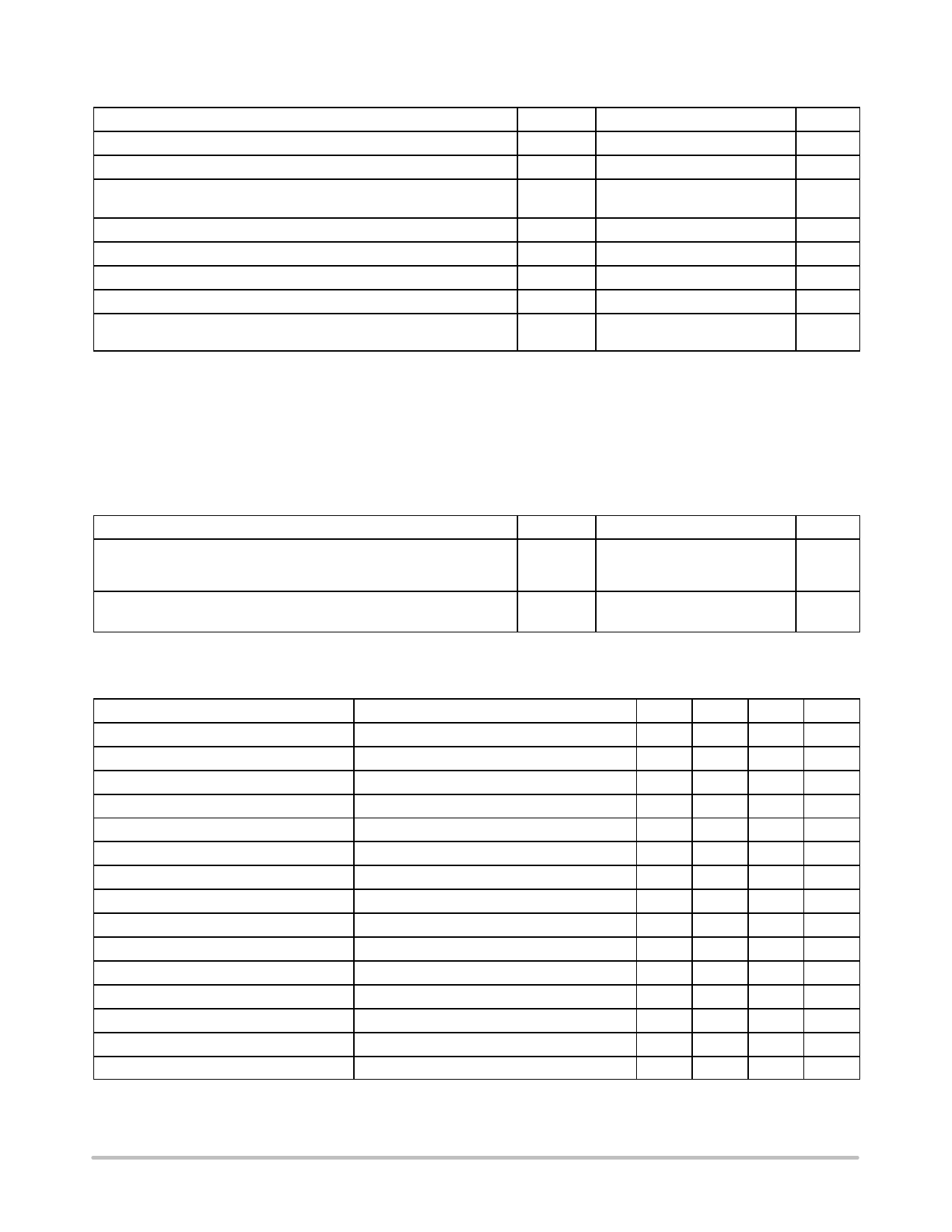
Table 3. ABSOLUTE MAXIMUM RATINGS
Rating
Symbol
Value
Unit
Supply Voltage Range
Vs
6.0 to 12 V
V
Input Voltage Range (Note 1)
Output Voltage Range
Vin
−0.3 to 6.0
V
Vout
−0.3 to 6.0 V or (Vin + 0.3),
V
whichever is lower
Maximum Junction Temperature
TJ(max)
140
°C
Storage Temperature Range
TSTG
−65 to 150
°C
ESD Capability, Human Body Model (Note 2)
ESDHBM
2
kV
ESD Capability, Machine Model (Note 2)
ESDMM
200
V
Lead Temperature Soldering
TSLD
260
°C
Reflow (SMD Styles Only), Pb−Free Versions (Note 3)
Stresses exceeding those listed in the Maximum Ratings table may damage the device. If any of these limits are exceeded, device functionality
should not be assumed, damage may occur and reliability may be affected.
1. Refer to ELECTRICAL CHARACTERISTICS and APPLICATION INFORMATION for Safe Operating Area.
2. This device series incorporates ESD protection and is tested by the following methods:
ESD Human Body Model tested per AEC−Q100−002 (EIA/JESD22−A114)
ESD Machine Model tested per AEC−Q100−003 (EIA/JESD22−A115)
Latchup Current Maximum Rating: v150 mA per JEDEC standard: JESD78
3. For information, please refer to our Soldering and Mounting Techniques Reference Manual, SOLDERRM/D
Table 4. THERMAL CHARACTERISTICS
Rating
Symbol
Value
Thermal Characteristics, QFN16, 3x3.3 mm (Note 4)
Thermal Resistance, Junction−to−Air (Note 5)
Thermal Reference, Junction−to−Lead2 (Note 5)
RqJA
RYJL
TBD
TBD
Thermal Characteristics, TSSOP−20 (Note 4)
Thermal Resistance, Junction−to−Air (Note 5)
RqJA
TBD
4. Refer to ELECTRICAL CHARACTERISTICS and APPLICATION INFORMATION for Safe Operating Area.
5. Values based on copper area of 645 mm2 (or 1 in2) of 1 oz copper thickness and FR4 PCB substrate.
Unit
°C/W
°C/W
Table 5. OPERATING RANGES (Note 6)
Parameter
Conditions
Min
Typ
Max Units
Operating Temperature
−40
85
C
IDD in typical power state
2.0
mA
Stimulus Generator Frequency
Tri−tone
3.1
3.4
kHz
SCR Trigger Current
8.0
mA
SCR Trigger output voltage
With 5 V supply
4.5
5.5
V
Fault Current Sensitivity
Programmable with CTresD
4.6
4.8
5.0
mA
Ground Fault Response Time
5 − 20 mA
150
ms
Ground Fault Response Time
20 − 40 mA
75
ms
Ground Fault Response Time
>40 mA
25
ms
Saturation Fault Response Time
>300 mA
1.4
ms
CT Turns Ratio
200
300
Ground – Neutral Detection Threshold
Total series impedance (Rn and Rg)
3.0
6.0
W
Internal Oscillator Frequency
2.0
MHz
CT Stimulus Current
Internally limited
1.0
mA
CT Driver Closed Loop BW
500
kHz
Product parametric performance is indicated in the Electrical Characteristics for the listed test conditions, unless otherwise noted. Product
performance may not be indicated by the Electrical Characteristics if operated under different conditions.
6. Refer to ELECTRICAL CHARACTERISTICS and APPLICATION INFORMATION for Safe Operating Area.
www.onsemi.com
4
Share Link: 