ESD7481MUT5G(2012) 데이터 시트보기 (PDF) - ON Semiconductor
부품명
상세내역
제조사
ESD7481MUT5G Datasheet PDF : 5 Pages
| |||
ESD7481MUT5G
Transient Voltage
Suppressors
Micro−Packaged Diodes for ESD Protection
The ESD7481 is designed to protect voltage sensitive components
that require ultra−low capacitance from ESD and transient voltage
events. Excellent clamping capability, low capacitance, low leakage,
and fast response time, make these parts ideal for ESD protection on
designs where board space is at a premium. Because of its low
capacitance, the part is well suited for use in high frequency designs
such as USB 2.0 high speed and antenna line applications.
Features
• Ultra−Low Capacitance 0.25 pF
• Low Clamping Voltage
• Small Body Outline Dimensions: 0.60 mm x 0.30 mm
• Low Body Height: 0.3 mm
• Stand−off Voltage: 5.0 V
• Low Leakage
• Insertion Loss: 0.030 dBm
• Response Time is < 1 ns
• Low Dynamic Resistance < 1 W
• IEC61000−4−2 Level 4 ESD Protection
• These Devices are Pb−Free, Halogen Free/BFR Free and are RoHS
Compliant
Typical Applications
• RF Signal ESD Protection
• RF Switching, PA, and Antenna ESD Protection
• Near Field Communications
http://onsemi.com
1
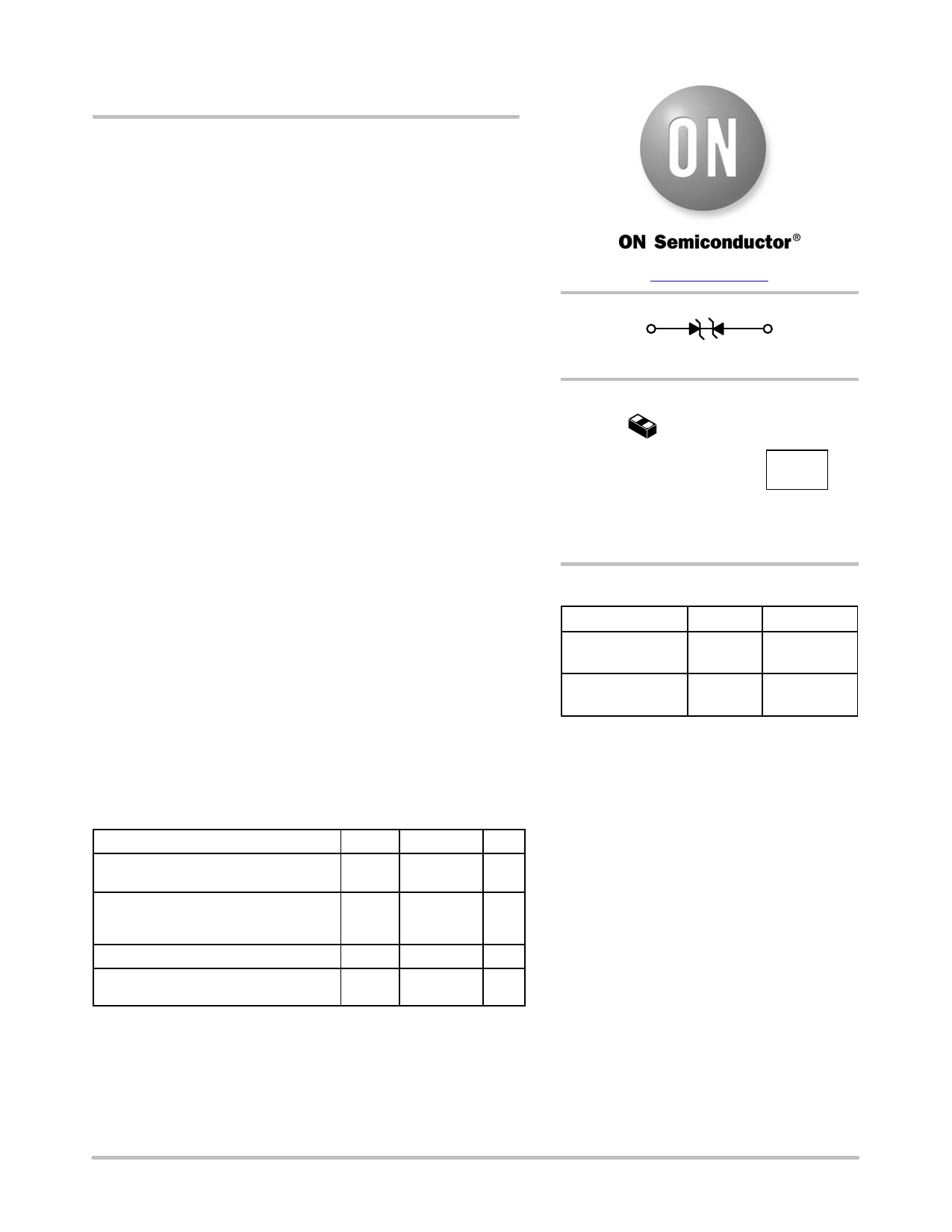
Cathode
2
Anode
X3DFN2
CASE 152AF
MARKING
DIAGRAM
PIN 1
M
F = Specific Device Code
(Rotated 90° clockwise)
M = Date Code
ORDERING INFORMATION
Device
Package
Shipping†
ESD7481MUT5G X3DFN2 5000/Tape & Reel
(Pb−Free)
†For information on tape and reel specifications,
including part orientation and tape sizes, please
refer to our Tape and Reel Packaging Specifications
Brochure, BRD8011/D.
MAXIMUM RATINGS
Rating
Symbol
Value
Unit
IEC 61000−4−2 (ESD)
Contact
Air
±20
kV
±20
Total Power Dissipation on FR−5 Board
(Note 1) @ TA = 25°C
Thermal Resistance, Junction−to−Ambient
Junction and Storage Temperature Range
Lead Solder Temperature − Maximum
(10 Second Duration)
°PD°
RqJA
TJ, Tstg
TL
250
mW
400
°C/W
−40 to +125 °C
260
°C
Stresses exceeding Maximum Ratings may damage the device. Maximum
Ratings are stress ratings only. Functional operation above the Recommended
Operating Conditions is not implied. Extended exposure to stresses above the
Recommended Operating Conditions may affect device reliability.
1. FR−5 = 1.0 x 0.75 x 0.62 in.
See Application Note AND8308/D for further description of survivability specs.
© Semiconductor Components Industries, LLC, 2012
1
September, 2012 − Rev. 2
Publication Order Number:
ESD7481/D
Share Link: 