74LV27 데이터 시트보기 (PDF) - NXP Semiconductors.
부품명
상세내역
제조사
74LV27 Datasheet PDF : 8 Pages
| |||
Philips Semiconductors
Triple 3-input NOR gate
Product data
74LV27
FEATURES
• Wide operating voltage: 1.0 to 5.5 V
• Optimized for Low Voltage applications: 1.0 to 3.6 V
• Accepts TTL input levels between VCC = 2.7 V and VCC = 3.6 V
• Typical VOLP (output ground bounce) < 0.8 V at VCC = 3.3 V,
Tamb = 25 °C.
• Typical VOHV (output VOH undershoot) > 2 V at VCC = 3.3 V,
Tamb = 25 °C.
• Output capability: standard
• ICC category: SSI
DESCRIPTION
The 74LV27 is a low-voltage Si-gate CMOS device and is pin and
function compatible with 74HC/HCT27.
The 74LV27 provides the 3-input NOR function.
QUICK REFERENCE DATA
GND = 0 V; Tamb = 25 °C; tr = tf ≤ 2.5 ns
SYMBOL
PARAMETER
CONDITIONS
tPHL/tPLH
Propagation delay
nA, nB, nC to nY
CL = 15 pF;
VCC = 3.3 V
CI
Input capacitance
CPD
Power dissipation capacitance per gate See Notes 1 and 2
NOTES:
1. CPD is used to determine the dynamic power dissipation (PD in µW)
PD = CPD × VCC2 × fi × N + Σ (CL × VCC2 × fo) where:
N = number of outputs switching;
fi = input frequency in MHz; CL = output load capacitance in pF;
fo = output frequency in MHz; VCC = supply voltage in V;
Σ (CL × VCC2 × fo) = sum of the outputs.
2. The condition is VI = GND to VCC.
TYPICAL
8
3.5
24
ORDERING INFORMATION
PACKAGES
14-Pin Plastic SO
TEMPERATURE RANGE
–40 °C to +125 °C
ORDER CODE
74LV27D
UNIT
ns
pF
pF
PKG. DWG. #
SOT108-1
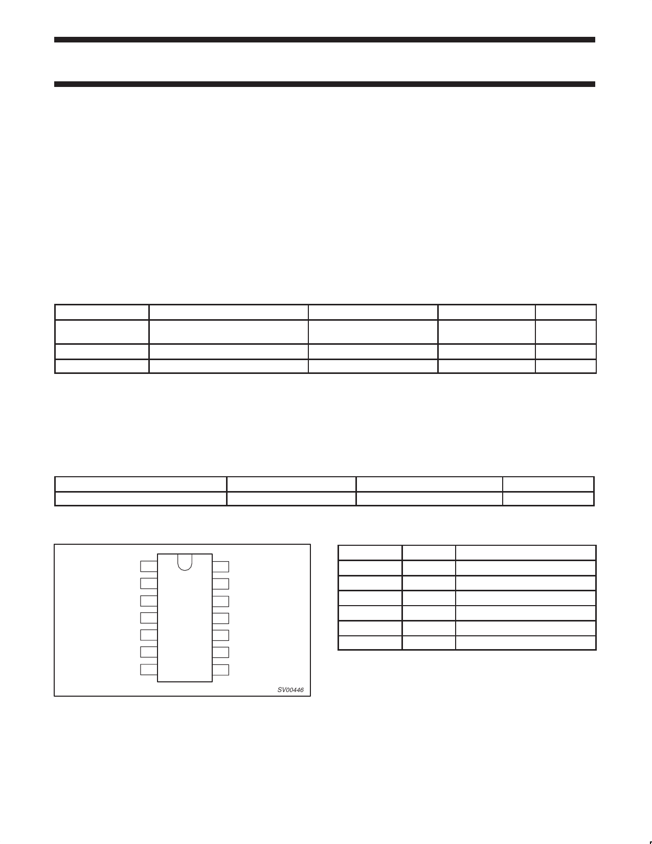
PIN CONFIGURATION
1A 1
1B 2
2A 3
2B 4
2C 5
2Y 6
GND 7
14 V CC
13 1C
12 1Y
11 3C
10 3B
9 3A
8 3Y
SV00446
PIN DESCRIPTION
PIN NUMBER SYMBOL
1, 3, 9
1A – 3A
2, 4, 10
1B – 3B
13, 5, 11
1C – 3C
7
GND
12, 6, 8
1Y – 3Y
14
VCC
NAME AND FUNCTION
Data inputs
Data inputs
Data inputs
Ground (0 V)
Data outputs
Positive supply voltage
2003 Mar 10
2
Share Link: 