ST9040Q1/XX 데이터 시트보기 (PDF) - STMicroelectronics
부품명
상세내역
제조사
ST9040Q1/XX Datasheet PDF : 56 Pages
| |||
ST9040
1.2 PIN DESCRIPTION
AS. Address Strobe (output, active low, 3-state).
Address Strobe is pulsed low once at the begin-
ning of each memory cycle. The rising edge of AS
indicates that address, Read/Write (R/W), and
Data Memory signals are valid for program or data
memory transfers. Under program control, AS can
be placed in a high-impedance state along with
Port 0 and Port 1, Data Strobe (DS) and R/W.
DS. Data Strobe (output, active low, 3-state). Data
Strobe provides the timing for data movement to or
from Port 0 for each memory transfer. During a
write cycle, data out is valid at the leading edge of
DS. During a read cycle, Data In must be valid prior
to the trailing edge of DS. When the ST9040 ac-
cesses on-chip memory, DS is held high during the
whole memory cycle. It can be placed in a high im-
pedancestate alongwith Port 0, Port 1, AS and R/W.
R/W. Read/Write (output, 3-state). Read/Write
determines the direction of data transfer for exter-
nal memory transactions. R/W is low when writing
to external program or data memory, and high for
all other transactions. It can be placed in a high im-
pedancestate along with Port 0, Port 1, AS and DS.
RESET. Reset (input, active low). The ST9 is initial-
isedby the Reset signal. With the deactivationof RE-
SET, program execution begins from the Program
memory location pointed to by the vector contained
in program memory locations 00h and 01h.
INT0, INT7. External interrupts (input, active on ris-
ing or falling edge). External interrupt inputs 0 and
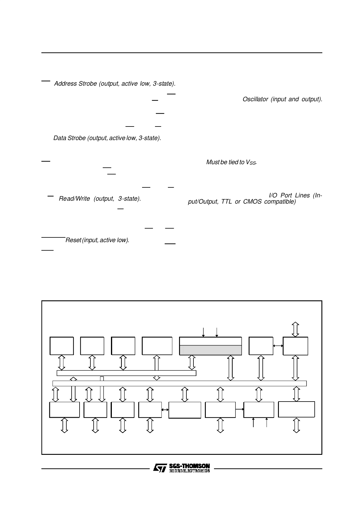
Figure 3. ST9040 Block Diagram
7 respectively. INT0 channel may also be used for
the timer watchdog interrupt.
OSCIN, OSCOUT. Oscillator (input and output).
These pins connect a parallel-resonant crystal
(24MHz maximum), or an external source to the
on-chip clock oscillator and buffer. OSCIN is the in-
put of the oscillator inverter and internal clock gen-
erator; OSCOUT is the output of the oscillator
inverter.
AVDD. AnalogVDD ofthe Analogto Digital Converter.
AVSS. Analog VSS of the Analog to Digital Con-
verter. Must be tied to VSS.
VDD. Main Power Supply Voltage (5V ± 10%)
VSS. Digital Circuit Ground.
P0.0-P0.7, P1.0-P1.7, P2.0-P2.7 P3.0-P3.7, P4.0-
P4.7, P5.0-P5.7, P7.0-P7.7 I/O Port Lines (In-
put/Output, TTL or CMOS compatible). 56 lines
grouped into I/O ports of 8 bits, bit programmable
under program control as general purpose I/O or
as alternate functions.
1.2.1 I/O Port Alternate Functions
Each pin of the I/O ports of the ST9040 may as-
sume software programmable Alternative Func-
tions as shown in the Pin Configuration Drawings.
Table 1-3 shows the Functions allocated to each
I/O Port pins and a summary of packagesfor which
they are available.
16k Bytes
ROM
512 Bytes
EEPROM
IN T0 INT7
256 Bytes
RAM
256 Bytes
REGISTER FILE
16-Bit TIMER / WATCHDOG + SPI
CPU
SCI
WITH DMA
8
I/O PORT 7
( SCI )
MEMORY BUS
REGISTER BUS
I/O PORT 0
( Address/Data )
I/O PORT 1
( Address )
I/O PORT 2
( SPI )
I/O PORT 3
( TIMERS )
8
8
8
8
2 x 16-bi t TIMER
W ITH DMA
I/O PORT 4
( Analog Inputs )
8
A/D
CONVERTER
I/O PORT 5
WITH HANDSHAKE
AVD D AVS S
8
V R0 0 1 3 85
6/56
®
Share Link: 