AD9731(RevA) 데이터 시트보기 (PDF) - Analog Devices
부품명
상세내역
제조사
AD9731 Datasheet PDF : 11 Pages
| |||
AD9731
PIN FUNCTION DESCRIPTION
Pin #
1
2–9
10
11
12, 13
14
15, 18, 28
16
17
19
20
21
22
23
24
25
26
27
Pin Name
D9(MSB)
D8–D1
D0(LSB)
CLOCK
NC
DIGITAL +VS
GND
DIGITAL –VS
RSET
ANALOG RETURN
IOUT
IOUTB
ANALOG –VS
REF IN
CONTROL AMP OUT
REF OUT
CONTROL AMP IN
DIGITAL –VS
Pin Description
Most significant data bit of digital input word.
Eight bits of 10-bit digital input word.
Least significant data bit of digital input word.
TTL-compatible edge-triggered latch enable signal for on-board registers.
No internal connection to this pin.
+5 V supply voltage for digital circuitry.
Converter Ground.
–5.2 V supply voltage for digital circuitry.
Connection for external reference set resistor; nominal 1.96 kΩ. Full-scale output current =
32 (Control Amp in V/RSET).
Analog Return. This point and the reference side of the DAC load resistors should be con-
nected to the same potential (nominally ground).
Analog current output; full-scale current occurs with a digital word input of all “1s.” With
external load resistor, output voltage = IOUT (RLOADʈRINTERNAL). RINTERNAL is nominally
240 Ω.
Complementary analog current output; full-scale current occurs with a digital word input
of all “0s.”
Negative analog supply, nominally –5.2 V.
Normally connected to CONTROL AMP OUT (Pin 24). Direct line to DAC current
source network. Voltage changes (noise) at this point have a direct effect on the full-scale
output current of the DAC. Full-scale current output = 32 (CONTROL AMP IN/RSET)
when using the internal amplifier. DAC load is virtual ground.
Normally connected to REF IN (Pin 23). Output of internal control amplifier which pro-
vides a reference for the current switch network.
Normally connected to CONTROL AMP IN (Pin 26). Internal voltage reference, nomi-
nally –1.25 V.
Normally connected to REF Out (Pin 25) if not connected to external reference.
Negative digital supply, nominally –5.2 V.
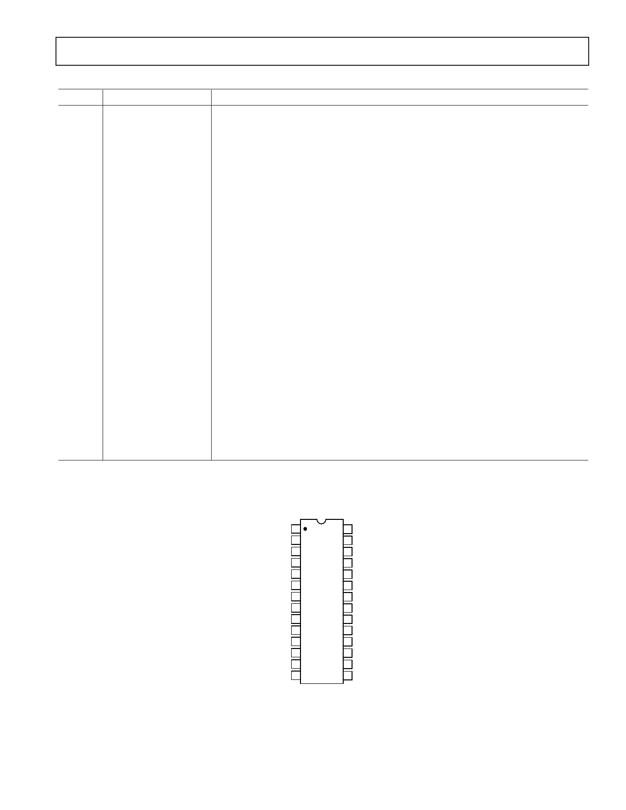
PIN CONFIGURATION
D9(MSB) 1
28 GND
D8 2
D7 3
27 DIGITAL –VS
26 CONTROL AMP IN
D6 4
25 REF OUT
D5 5
24 CONTROL AMP OUT
D4 6 AD9731 23 REF IN
D3 7 TOP VIEW 22 ANALOG –VS
D2 8 (Not to Scale) 21 IOUTB
D1 9
20 IOUT
D0(LSB) 10
19 ANALOG RETURN
CLOCK 11
18 GND
NC 12
NC 13
DIGITAL +VS 14
17 RSET
16 DIGITAL –VS
15 GND
NC = NO CONNECT
REV. A
–5–
Share Link: 