AD7249 데이터 시트보기 (PDF) - Analog Devices
부품명
상세내역
제조사
AD7249 Datasheet PDF : 14 Pages
| |||
AD7249
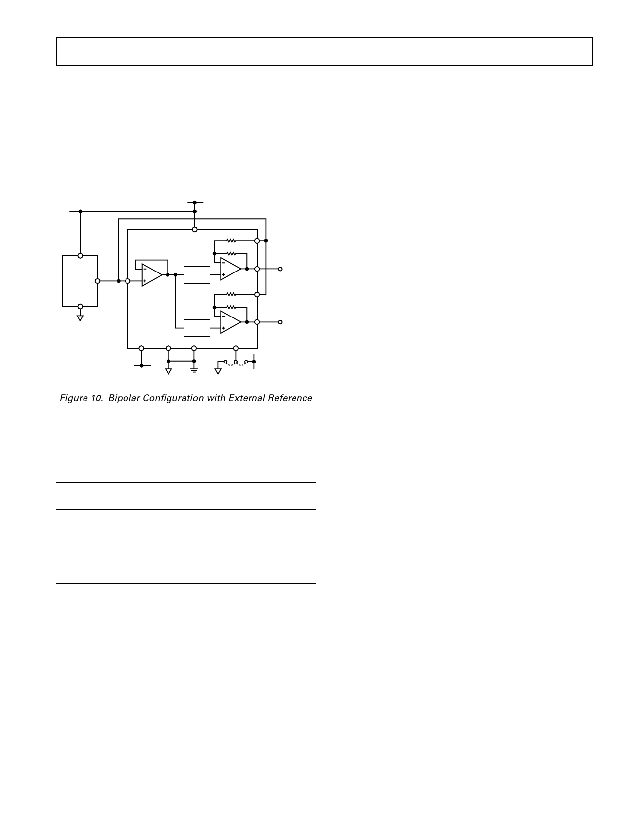
Bipolar (؎5 V) Configuration
The bipolar configuration for the AD7249, which gives an out-
put range of –5 V to +5 V, is achieved by connecting ROFSA,
ROFSB to VREFIN. The AD7249 must be operated from dual
supplies to achieve this output voltage range. Either offset binary
or twos complement coding may be selected. Figure 10 shows
the connection diagram for bipolar operation. An AD586 pro-
vides the reference voltage for the DAC but this could be pro-
vided by the on-chip reference by connecting REFOUT to
REFIN.
VDD
VDD
2R
+VIN
AD7249*
2R
AD586
VOUT
REFIN
12-BIT
A1
DAC A
2R
2R
ROFSA
VOUTA
–5V TO +5V
ROFSB
12-BIT
A2
DAC B
VOUTB
–5V TO +5V
VSS AGND DGND BIN/COMP
VSS
VDD
*ADDITIONAL PINS OMITTED FOR CLARITY.
Figure 10. Bipolar Configuration with External Reference
Bipolar Operation (Twos Complement Data Format)
The AD7249 is configured for twos complement data format
by connecting BIN/COMP (Pin 7) high. The analog output vs.
digital code is shown in Table II.
Table II. Twos Complement Bipolar Code Table
Input Data Word
MSB LSB
XXXY 0111 1111 1111
XXXY 0000 0000 0001
XXXY 0000 0000 0000
XXXY 1111 1111 1111
XXXY 1000 0000 0001
XXXY 1000 0000 0000
Analog Output, VOUT
+REFIN × (2047/2048)
+REFIN × (1/2048)
0V
–REFIN × (1/2048)
–REFIN × (2047/2048)
–REFIN × (2048/2048) = –REFIN
X = Don’t Care.
Y = DAC Select Bit, 0 = DAC A, 1 = DAC B.
Note: 1 LSB = REFIN/2048.
Bipolar Operation (Offset Binary Data Format)
The AD7249 is configured for Offset Binary data format by
connecting BIN/COMP (Pin 7) low. The analog output vs.
digital code may be obtained by inverting the MSB in Table II.
APPLYING THE AD7249
Good printed circuit board layout is as important as the overall
circuit design itself in achieving high speed converter perfor-
mance. The AD7249 works on an LSB size of 2.44 mV for the
unipolar 0 V to 10 V range and the bipolar ± 5 V range, when
using the unipolar 0 V to 5 V range the LSB size is 1.22 mV.
Therefore the designer must be conscious of minimizing noise in
both the converter itself and in the surrounding circuitry.
Switching mode power supplies are not recommended as switch-
ing spikes can feedthrough to the on-chip amplifier. Other causes of
concern are ground loops and feedthrough from microproces-
sors. These are factors which influence any high performance
converter, and proper printed circuit board layout which mini-
mizes these effects is essential to obtain high performance.
LAYOUT HINTS
Ensure that the layout has the digital and analog tracks sepa-
rated as much as possible. Take care not to run any digital track
alongside an analog signal track. Establish a single point analog
ground separate from the logic system ground. Place this star
ground as close as possible to the AD7249. Connect all analog
grounds to this star point and also connect the AD7249 DGND
pin to this point. Do not connect any other digital grounds to
this analog ground point. Low impedance analog and digital
power supply common returns are essential for low noise opera-
tion of high performance converters. To accomplish this track
widths should be kept a wide as possible and also the use of
ground planes minimizes impedance paths and also guards the
analog circuitry from digital noise.
NOISE
Keep the signal leads on the VOUTA and VOUTB signals and the
signal return leads to AGND as short as possible to minimize
noise coupling. In applications where this is not possible use a
shielded cable between the DAC outputs and their destination.
Reduce the ground circuit impedance as much as possible since
any potential difference in grounds between the DAC and its
destination device appears as an error voltage in series with the
DAC output.
Power Supply Decoupling
To achieve optimum performance when using the AD7249, the
VDD and VSS lines should be decoupled to AGND using 0.1 µF
capacitors. In noisy environments it is recommended that 10 µF
capacitors be connected in parallel with the 0.1 µF capacitors.
REV. D
–9–
Share Link: 