AP1122DG-13 데이터 시트보기 (PDF) - Diodes Incorporated.
부품명
상세내역
제조사
AP1122DG-13 Datasheet PDF : 11 Pages
| |||
AP1122
1A LOW DROPOUT POSITIVE REGULATOR
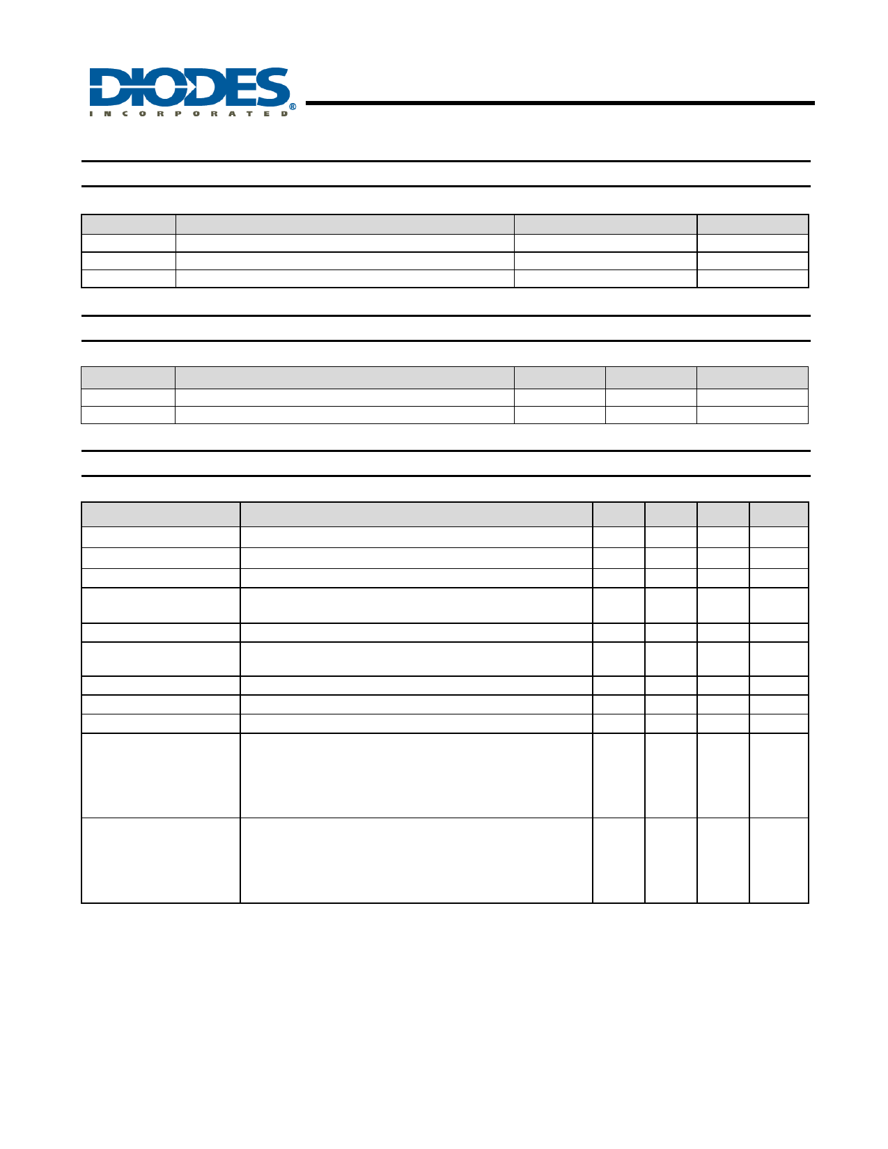
Absolute Maximum Ratings
Symbol
VIN
TST
TMJ
Parameter
DC Supply Voltage
Storage Temperature
Maximum Junction Temperature
Recommended Operating Conditions
Rating
-0.3 to 12
-65 to +150
150
Symbol
IOUT
TOP
Parameter
Output Current
Operating Junction Temperature Range
Min
Max
-
1.0
0
125
Electrical Characteristics (Under Operating Conditions)
Unit
V
oC
oC
Unit
A
oC
Parameter
Output Voltage
Line Regulation
Load Regulation
Dropout Voltage
(VIN-VOUT)
Current Limit
Minimum Load Current
(Note 4)
Thermal Regulation
Ripple Rejection
Temperature Stability
θJA Thermal Resistance
Junction-to-Ambient
θJC Thermal Resistance
Junction-to-Case
Test Conditions
2.5V≦VIN≦12V, IO=10mA, TA=25oC
2.5V≦VIN≦12V, IO=10mA, TA=25oC
VIN=2.5V~12V, 10mA<Io<1A, TA=25oC (Note 2, 3)
IOUT = 1A ,ΔVOUT = 1%VOUT
(VIN-VOUT) = 5V
0oC≦TJ≦125oC
TA=25oC, 30ms pulse
F=120Hz,COUT=25uF Tantalum, IOUT=1A, VIN=VOUT+3V
IO=10mA
SOT89-3L: Control Circuitry/Power Transistor (Note 5)
SOT223-3L: Control Circuitry/Power Transistor (Note 6)
TO252-3L: Control Circuitry/Power Transistor (Note 5)
TO220-3L: Control Circuitry/Power Transistor (Note 5)
TO263-3L: Control Circuitry/Power Transistor (Note 5)
SOT89-3L: Control Circuitry/Power Transistor (Note 5)
SOT223-3L: Control Circuitry/Power Transistor (Note 6)
TO252-3L: Control Circuitry/Power Transistor (Note 5)
TO220-3L: Control Circuitry/Power Transistor (Note 5)
TO263-3L: Control Circuitry/Power Transistor (Note 5)
Min
1.176
Typ.
1.2
Max
1.224
0.2
1
1.3
1. 1
5
10
0.008 0.04
60
70
0.5
182
107
73
78
60
42
16
12
3.5
3.5
Unit
V
%
%
V
A
mA
%/W
dB
%
oC/W
oC/W
Notes:
2. See thermal regulation specifications for changes in output voltage due to heating effects. Line and load regulation are
measured at a constant junction temperature by low duty cycle pulse testing. Load regulation is measured at the output lead
= 1/18” from the package.
3. Line and load regulation are guaranteed up to the maximum power dissipation of 15W. Power dissipation is determined by the
difference between input and output differential and the output current. Guaranteed maximum power dissipation will not be
available over the full input/output range.
4. Quiescent current is defined as the minimum output current required in maintaining regulation. At 12V input/output differential
the device is guaranteed to regulate if the output current is greater than 10mA.
5. Test conditions for SOT89-3L, TO252-3L, TO220-3L, and TO263-3L: Devices mounted on FR-4 substrate, single sided PC
board, 2oz copper, with minimum recommended pad layout, no air flow.
6. Test condition for SOT223-3L: Device mounted on FR-4 substrate, single sided PC board, 2oz copper, with 5mmX5mm thermal
pad layout, no air flow.
AP1122
Document number: DS31012 Rev. 9 - 2
3 of 11
www.diodes.com
May 2010
© Diodes Incorporated
Share Link: 