LC709006A-E 데이터 시트보기 (PDF) - ON Semiconductor
부품명
상세내역
제조사
LC709006A-E Datasheet PDF : 14 Pages
| |||
LC709006A
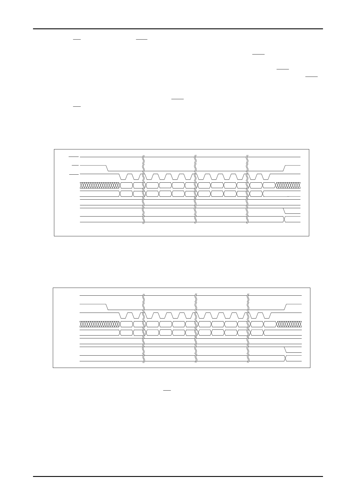
(2) Data communication mode
1) When the CS pin is set low with the RES pin held high, the LC709006A gets ready for serial communication.
(Subsequently, processing in steps 2) and 3) are identical to steps 2) and 3) in paragraph (1)-2).
2) The input data at P00 is sent directly to the DOUT pin on the first falling edge of the CLK signal. Data at pins
P01 to P27 is loaded into the shift register on the next rising edge of the clock.
3) Subsequently, the ports' input data, which is loaded into the shift register on the falling edge of CLK, is placed at
the DOUT pin sequentially (P00→P07, P10→P17, P20→P27) in synchronization with the falling edges of CLK,
starting at port pin P00. In parallel with this operation, when data to be placed at the ports is supplied to the DIN
pin sequentially starting at the port pin P00 (P00→P07, P10→P17, P20→P27), it is loaded into the internal shift
register in synchronization with the rising edges of CLK.
4) When the CS pin is set high after the rising edge of the 24th clock, the data loaded in the shift register is loaded
into the DDR register which determines the output state of the ports and the states of all port pins (P00 to P27) are
then changed (output) according to the conditions established in the DDR and DTR registers. Serial data that
occurs following the initial communication mode processing is always loaded into the DTR register.
RES
CS
CLK
DIN
0
1
6
7
8
9
14 15
16 17
22 23
P00_DO P01_DO P06_DO P07_DO P10_DO P11_DO P16_DO P17_DO P20_DO P21_DO P26_DO P27_DO
DOUT
DDR
P27_DI(Previous Data)
P00_DI P01_DI P06_DI P07_DI P10_DI P11_DI P16_DI P17_DI P20_DI P21_DI P26_DI
P27_DI
DTR
P00 to P27
Hi-Z
Hi-Z
Hi-Z
Hi-Z
P00-P27_OUT
* PXX_DO denotes the output data to the port pin identified by PXX.
Fig. 3
5) Subsequently, the state of all port pins (P00 to P27) is updated each time the set of steps 1) to 4) described in
paragraph (2) are performed.
RES
CS
CLK
DIN
DOUT
DDR
DTR
P00 to P27
0
1
6
7
8
9
14
15
16 17
22
23
P00_DO P01_DO P06_DO P07_DO P10_DO P11_DO P16_DO P17_DO P20_DO P21_DO P26_DO P27_DO
P27_DI(Previous Data)
P00_DI P01_DI
P06_DI P07_DI P10_DI P11_DI
P16_DI P17_DI P20_DI P21_DI
P26_DI
P27_DI
P00-P27_OUT(Previous Data)
P00-P27_OUT(Previous Data)
P00-P27_OUT(Previous Data)
P00-P27_OUT(Previous Data) P00-P27_OUT
Fig. 4
Note: Connect a Pull-up resister (about 100kΩ) to CS using MCU VDD.
No.8265-10/14
Share Link: 